
The terrain for designing circuit boards for medical devices in Australia has changed dramatically. Effective May 2026, the TGA has moved from merely suggesting best cybersecurity practices to demanding comprehensive, hardware-based security measures. This implies that security-by-design is not a catchy marketing phrase any more – but rather an obligatory requirement.
At Circuit Board Design, We have noticed that there is a very important trend that has emerged – that the TGA is focusing more on the physical hardware layer and identifying it as the point of weakness. The fact that software-level encryption may not be enough because the hardware itself can be accessed by debug headers and side-channel attacks should be taken into consideration in order to comply with the TGA medical standard.
The Physics of Hardware Vulnerability
In medical electronics, the “physics” associated with a cybersecurity threat may be associated with electrical signal manipulation at the board level. An adversary seeking to compromise the integrity of medical devices, such as an insulin pump, a pacemaker, or diagnostic gateways, usually targets three physical vectors:
Firmware Injection: Using the JTAG or SWD header to stop CPU processing and inject malicious firmware into the device.
Intercepting Communication: Investigating open SPI or I2C bus channels to extract patient information and cryptographic keys transferred between the MCU and off-board RAM.
Exploiting Side-Channels: Examining power signatures or electromagnetic emanations to deduce encryption keys.
When developing for Australia, where devices must function in decentralized or rural settings (e.g., NB-IoT remote diagnostics in rural hospitals), the physical attack surface is greatly increased. Common PCB design techniques like leaving debug pads accessible or
The TGA’s 2026 Landscape: From Software to Silicon
According to the recently updated Cyber Security Guidance for Industry from the TGA, the Root of Trust should be based in silicon. Unlike previous versions of the Needed Principles, which considered software patching and SBOM management, the requirements of the year 2026 demand that there must be proof that the device cannot be tampered with by an actor who is physically close.
It reflects a general trend seen across IEC 81001-5-1 compliance where hardware is viewed as a key component of the entire security chain, as without it, software cannot be trusted either. Medical device pcb design therefore requires the implementation of particular hardware components that will ensure the impossibility of any unauthorized code execution or data breaches.
Hardware Root of Trust (RoT): The Silicon Anchor
The most significant requirement under the new TGA framework is the implementation of a Hardware Root of Trust (RoT). This is typically achieved through an integrated Hardware Security Module (HSM) or a Secure Element (SE).
An HSM is a dedicated, tamper-resistant microchip that manages cryptographic keys and performs secure computations. In a medical context, the HSM serves several critical functions:
Key Isolation: Private keys never leave the secure boundary of the HSM. Even if the main application processor is compromised, the attacker can't extract the underlying cryptographic material.
True Random Number Generation (TRNG): Providing high-entropy seeds for encryption, preventing predictable key generation.
Secure Storage: Protecting critical device identity certificates used for TGA-mandated secure updates.
At Circuit Board Design, we integrate components like the Microchip ATECC608B or NXP SE050 directly into the schematic capture phase, ensuring that the I2C/SPI bus connecting the HSM to the MCU is shielded and optimized for signal integrity.
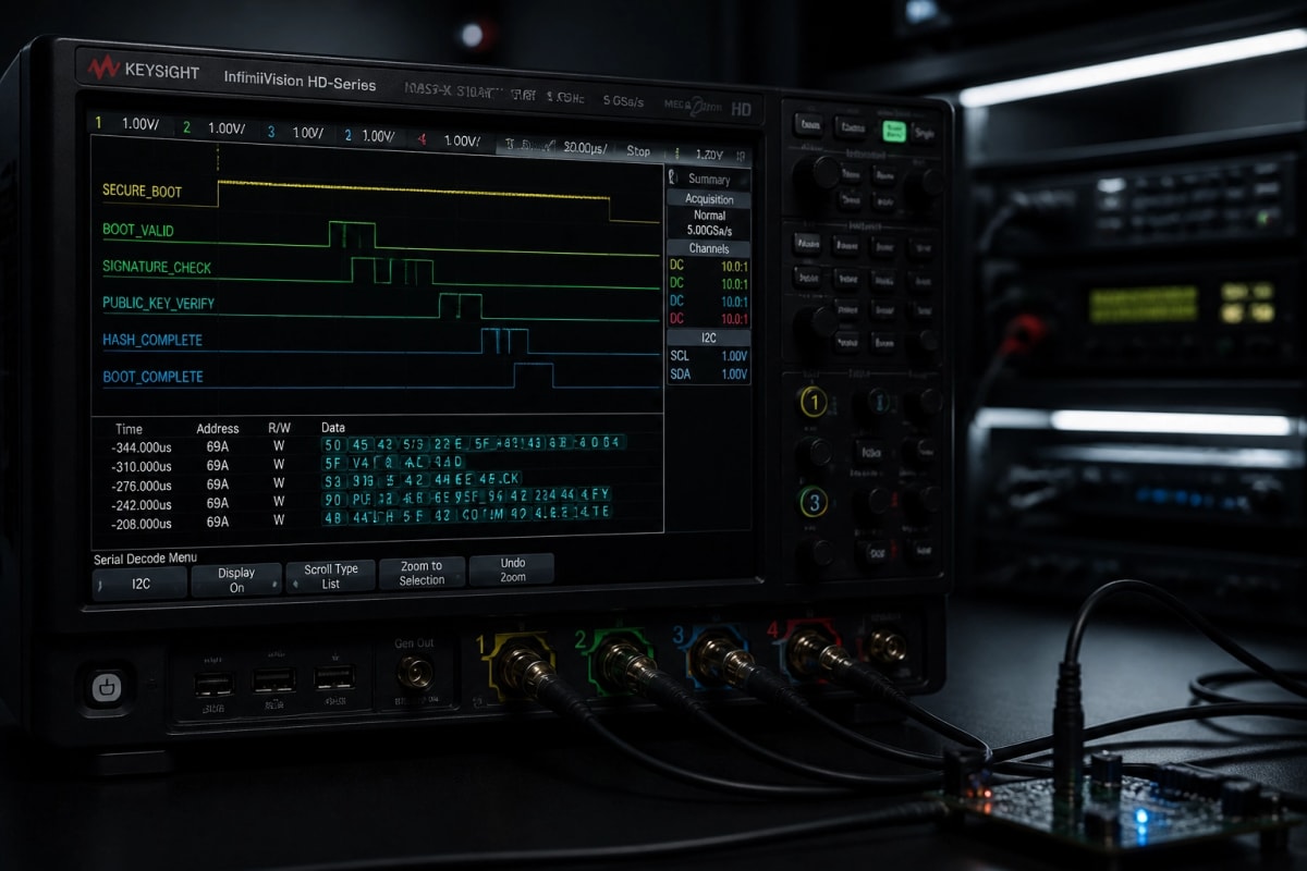
Oscilloscope visualization of a cryptographically signed secure boot pulse sequence, ensuring only authorized firmware is executed.
The Mechanics of Secure Boot Architecture
Secure Boot is the process by which a medical device validates the digital signature of its firmware before execution. The TGA now requires that this process be "immutable": meaning the initial bootloader code must be stored in Read-Only Memory (ROM) or write-protected flash that can't be altered by software.
The sequence follows a strict cryptographic chain:
Power-On: The MCU executes the primary bootloader from internal ROM.
Validation: The primary bootloader uses the public key stored in the HSM to verify the signature of the secondary bootloader (SBL).
Execution: Only if the signature matches does the SBL load the main application firmware.
If any link in this chain is broken: due to a firmware update being tampered with or a malicious actor attempting to load a custom OS: the device will enter a "Secure Fault" state and refuse to boot. This prevents the "bricking" of medical devices by ransomware or the unauthorized modification of therapy delivery parameters.
Debug Port Obfuscation: Hiding the Backdoor
One of the most common vulnerabilities in medical PCBs is the presence of unpopulated JTAG or SWD headers. While needed for R&D and factory testing, these ports are "gold mines" for reverse engineers. The TGA now expects manufacturers to provide evidence of "Debug Port Deactivation or Obfuscation."
In our multi-layer PCB layout process, we employ several "The Right Way" strategies for port protection:
Physical Masking: Placing debug pads under BGA components or within inner layers accessible only via specialized "blind" vias.
Logic-Based Locking: Implementing a password-protected JTAG gatekeeper. The port remains electrically inert until a specific cryptographic challenge-response is completed.
Resistor Array Obfuscation: Using 0201 or 01005 resistor networks in a non-standard configuration to "scramble" the JTAG pinout. To an external observer, the pads look like standard decoupling or pull-up resistors.
Permanent Disabling: Using eFuses to permanently blow the debug circuitry once the device leaves the manufacturing support phase.
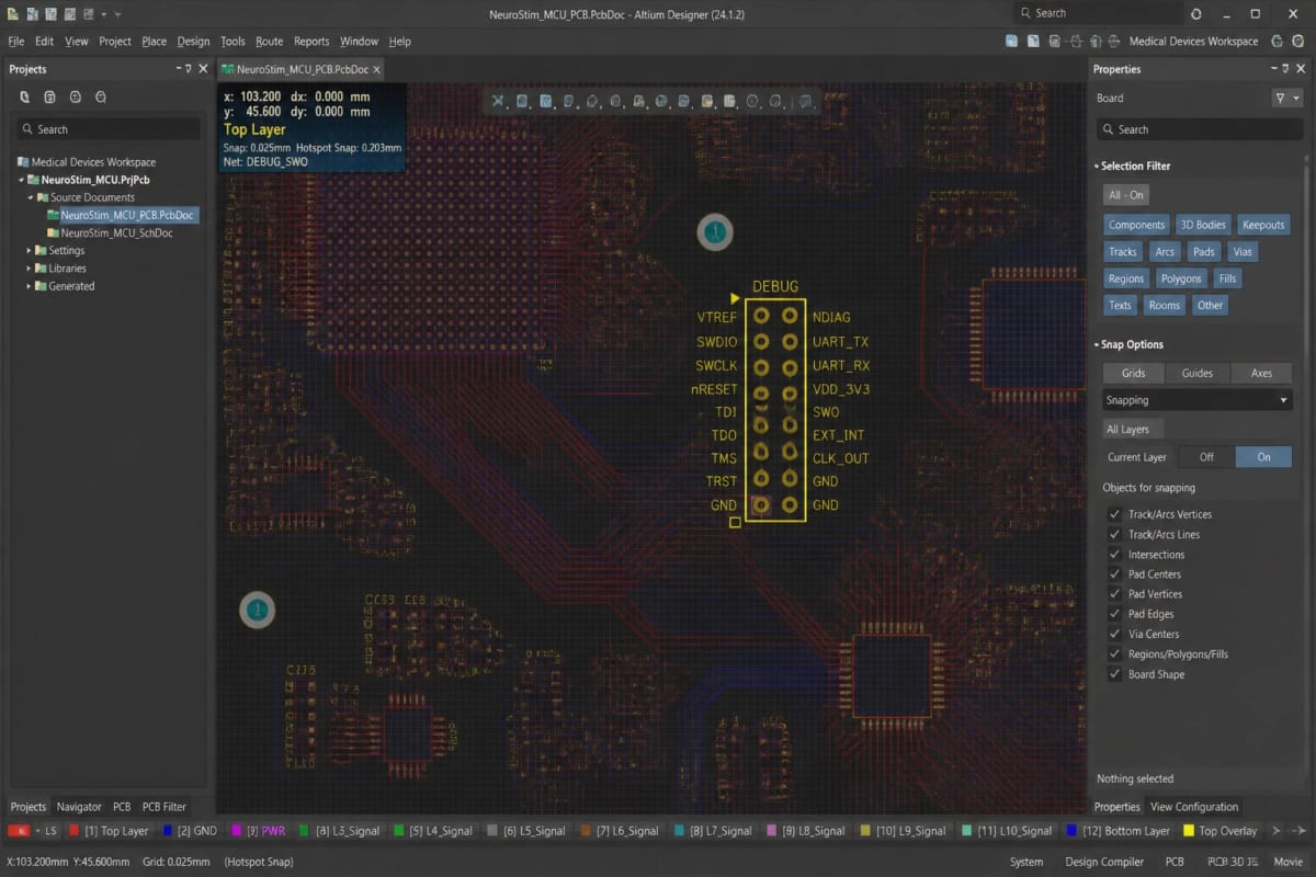
A professional 12-layer medical PCB layout in Altium Designer showing obfuscated routing patterns and hidden debug vias to prevent unauthorized physical access.
Physical Anti-Tamper: The Active Mesh Defense
For high-risk devices (Class III), the TGA is increasingly interested in physical anti-tamper measures. These are features that detect if a device's enclosure has been opened or if the PCB has been probed.
Active Mesh Layers
An active mesh is a fine grid of traces woven into the outer layers of the PCB. A low-power security controller constantly monitors the continuity and capacitance of this mesh. If a drill bit or a probe breaks a trace or even changes the dielectric constant by getting too close, the controller triggers an immediate "Zeroize" command, wiping all sensitive keys from the HSM.
Light and Pressure Sensors
Integrating miniature ambient light sensors (ALS) inside a light-tight enclosure can detect if the "lid is popped." Similarly, board-mounted pressure sensors can detect the change in atmospheric pressure if a vacuum-sealed medical enclosure is breached. These triggers are integrated at the hardware level, ensuring they function even if the main CPU is in a sleep state.
Comparison: Legacy vs. TGA-Compliant Medical PCB Design
The following table outlines the fundamental differences in engineering requirements before and after the 2026 cybersecurity mandate.
| Feature | Legacy Medical PCB Design | TGA-Compliant (2026) Design | | :--- | :--- | :--- | | Root of Trust | Software-based (Flash storage) | Hardware-anchored (HSM / Secure Element) | | Boot Sequence | Unsigned or simple checksum | Cryptographically signed Secure Boot | | Debug Headers | Standard 10-pin headers (unpopulated) | Obfuscated, encrypted, or eFuse-disabled | | Firmware Updates | Over-the-Air (OTA) without validation | Signed OTA with rollback protection | | Bus Communication | Clear-text SPI/I2C | Encrypted/Authenticated bus protocols | | Physical Protection | Plastic enclosure screws | Active mesh / Tamper-evident seals | | Component Selection | Standard industrial MCUs | MCUs with TrustZone / Secure Enclaves |
Schematic Phase Integration: Security as a First-Class Citizen
The most expensive mistake in medical device pcb design is treating security as an afterthought. If you reach the testing & validation phase and discover your hardware lacks a secure boot anchor, the resulting redesign can cost hundreds of thousands of dollars in TGA re-submission fees.
Security must begin during schematic capture. This involves:
Defining the Trust Boundary: Identifying which components handle sensitive data (Patient Health Information - PHI) and isolating them from "untrusted" peripherals like Bluetooth or Wi-Fi modules.
Power Domain Isolation: Ensuring the HSM has a dedicated, filtered power rail to prevent "Power Analysis" side-channel attacks.
Trace Shielding: Using ground planes and "stitching vias" to shield sensitive data buses from electromagnetic sniffing.
Our engineers use Altium Designer’s advanced constraint management to ensure that secure traces are never routed near the board edge or near high-power components like a BMS design module where noise could be used to mask a side-channel attack.
!Active Anti-Tamper Mesh Macro visualization of an active anti-tamper mesh on a PCB inner layer, designed to detect physical probing or drilling.
Harsh Environments and Regional Compliance
In Australia, medical devices are often deployed in regional areas where they face "mineral dust migration" and "night-day condensation cycles." While these seem like purely mechanical issues, they have profound security implications.
Corrosion or dust accumulation on a debug port can cause "floating pins" that might inadvertently put a device into a test mode or factory reset state. We mandate conformal coating for all regional Australian deployments: not just for longevity, but to maintain the electrical integrity of the security circuits. A compromised dielectric due to moisture can lead to false tamper triggers or, worse, the failure of a secure boot sequence.
FAQ: TGA Medical PCB Security
What is the difference between TGA and FDA cybersecurity requirements?
While both emphasize risk management, the TGA has specific requirements regarding the "Sovereign capability" of the data. For Australian medical devices, there's a higher emphasis on local data residency and the ability for the device to operate securely in remote, low-bandwidth environments using protocols like NB-IoT.
Does a simple password on my firmware protect me?
No. Standard firmware passwords can often be bypassed by dumping the flash memory directly from the chip. TGA compliance requires that the firmware be encrypted and that the decryption key be stored in a hardware-protected enclave (HSM).
How does Secure Boot affect manufacturing?
Secure Boot requires a "Key Injection" step during production. You must have a secure way to load your private keys into the HSM at the factory. We assist our clients in setting up secure manufacturing flows to ensure keys are never exposed to the contract manufacturer (CM).
Is obfuscation really necessary if I use an HSM?
Yes. Defense-in-depth is a core tenet of TGA auditing. An HSM protects keys, but an exposed debug port might still allow an attacker to read out non-encrypted memory or perform a Denial of Service (DoS) attack on the device's therapeutic functions.
Moving to Production with Confidence
Navigating the TGA's cybersecurity mandate requires a multidisciplinary approach that blends physics, cryptography, and advanced PCB engineering. At Circuit Board Design, we specialize in taking complex medical concepts from the schematic phase to a TGA-ready, manufactured product.
Whether you're building a wearable biosensor or a high-power clinical diagnostic tool, our IPC CID+ certified engineers ensure your hardware isn't just functional, but fortified. By integrating HSMs, secure boot architectures, and physical anti-tamper measures into your medical device pcb design, we help you move from a vulnerable prototype to a compliant, market-ready medical solution.
Contact us today at hello@circuit-board-design.com to discuss your TGA compliance roadmap and secure your hardware against the threats of 2026 and beyond.
About the author
Niloy is an IPC CID+ certified PCB design engineer and founder of Electuni LLC, delivering custom PCB design, embedded systems, and hardware prototypes to clients across North America, Europe, the Caribbean, and South Asia. Specialties: Altium Designer, KiCad, energy metering ICs (ATM90E36A), battery management (TI BQ-series), and ESP32/STM32 firmware.


