
7 Mistakes You’re Making with PCB Layout (And How to Fix Them for a 99.7% Yield Rate)
You are standing in the assembly bay, the hum of the pick-and-place machine a rhythmic background to the cold knot of dread tightening in your stomach. The first batch of boards from the prototype run has just emerged from the reflow oven, and the result is catastrophic.
Half of your passive components are standing on end like tiny, ceramic monoliths: a phenomenon known as tombstoning. The high-stakes project you’ve spent months meticulously crafting is now bleeding capital. Every hour of delay evaporates your market share, and the prospect of manual rework brings a specific kind of heartburn only a hardware engineer understands.
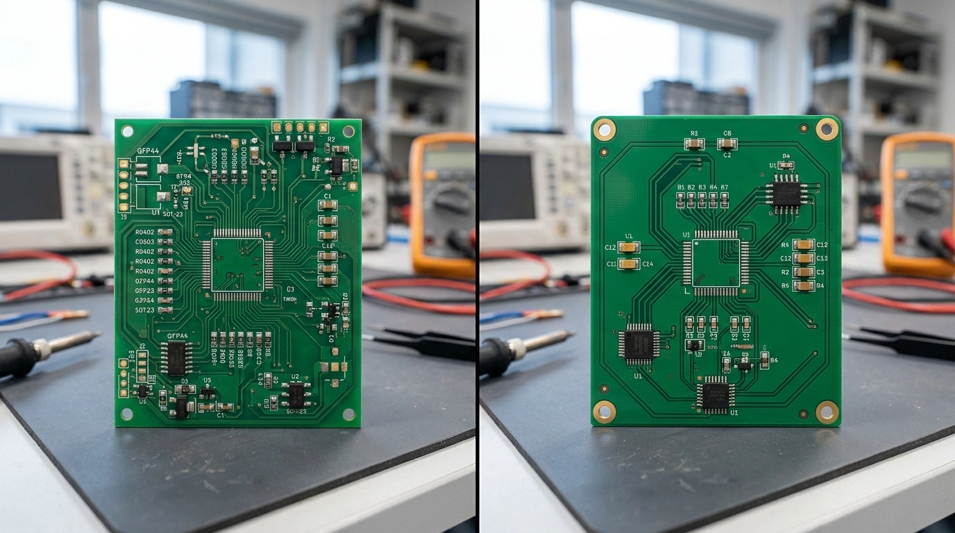
This isn't just bad luck. It is the harsh physical reality of a layout that failed to bridge the gap between a theoretical schematic and a metallurgical process. At Circuit Board Design, we specialize in preventing these "nightmare" scenarios. By adhering to a rigorous methodology that ensures high reliability pcb design, we maintain a 99.7% first-pass yield rate.
Here are the seven most insidious mistakes currently sabotaging your yield: and the clinical fixes required to rectify them.
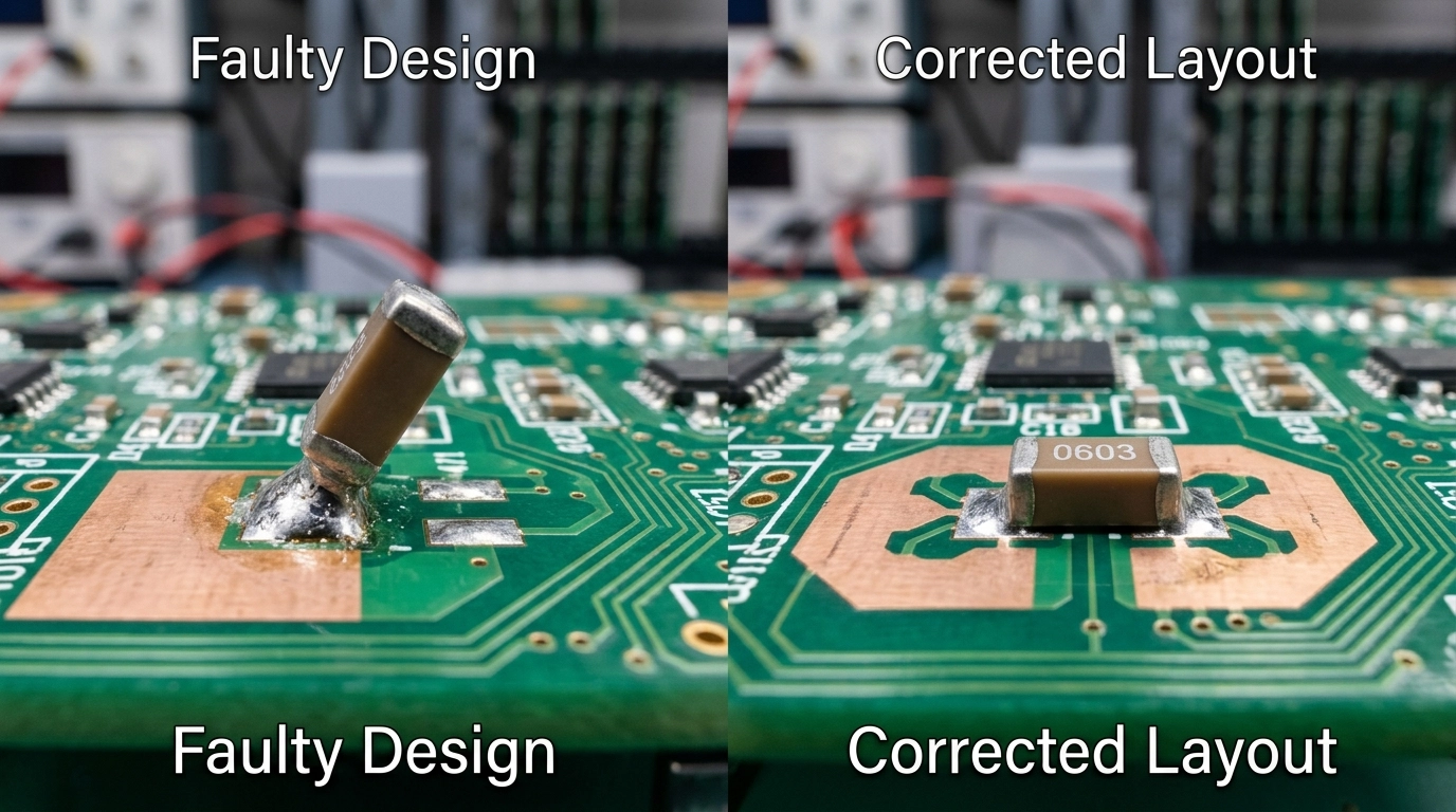
1. The Physics of Thermal Imbalance: The Tombstone Effect
The most common psychological reflex for a designer is to focus on connectivity while ignoring thermodynamics. When one pad of a small SMD component is connected to a massive ground plane and the other to a thin signal trace, a thermal gradient is born.
During reflow, the solder on the pad with less copper mass liquefies first. The surface tension of this molten solder pulls on the component. Without an equal and opposite pull from the other pad, the component is yanked upright. The tombstone is set, and the board has failed.
The Fix: Implement thermal relief traces for all connections to large copper pours. Ensuring symmetrical heat distribution across pads is not an aesthetic choice; it is a metallurgical necessity. For a deeper dive, see our complete guide to preventing the tombstone effect.
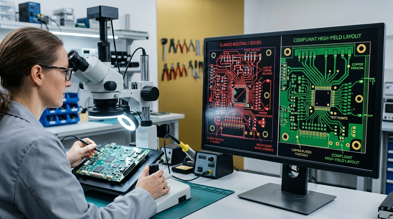
2. The Insidious Chemistry of Acid Traps
In the pursuit of compact PCB layout design services, designers often employ acute angles in their trace routing. This is a fundamental error. During the etching process, chemicals can become trapped in these sharp nooks.
This trapped etchant continues to eat away at the copper long after the board has left the chemical bath, leading to "insidious" open circuits that may not fail until the product is in the customer’s hands.
The Fix: Never use angles sharper than 90 degrees; 45-degree mitered corners are the industry standard for a reason. In our PCB design services, we utilize automated DRC (Design Rule Check) scripts to flag any trace geometry that could harbor residual chemicals, ensuring long-term reliability.
3. Mechanical Stress and the "Dead Zone" of Edge Clearance
Copper traces or components placed too close to the board edge are living on borrowed time. During depanelization: the process of breaking individual boards from a larger panel: the PCB undergoes significant mechanical stress.
If a ceramic capacitor is located within the "stress zone" (typically within 50-75 mils of the edge), it can develop micro-fractures. These aren't visible to the naked eye, but they will eventually lead to a short circuit or a total system failure.
The Fix: Maintain a strict "no-fly zone" for all sensitive components near the board edge. For high-reliability designs, we mandate a minimum clearance of 125 mils for larger components to account for mechanical flexure during handling.
4. The Vision Gap: Neglecting Fiducial Marks
Modern assembly is a feat of robotic precision, but robots are only as good as their vision systems. If your layout lacks clear, high-contrast fiducial marks, the pick-and-place machine is essentially flying blind.
Without these global and local reference points, component offsets become inevitable. A 0.5mm pitch BGA misaligned by even a fraction of a millimeter results in a bridge that is nearly impossible to fix without expensive X-ray inspection and rework.
The Fix: Place three global fiducials on the corners of your board and local fiducials for every fine-pitch IC. This allows for the sub-micron alignment required to hit our 48-hour turnaround time without sacrificing precision.
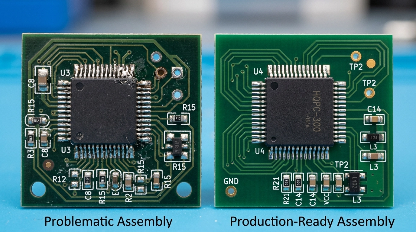
5. The Solder Siphon: Via-in-Pad Without Plugging
In high-density designs, placing a via directly on a component pad is a common tactic to save space. However, if that via is not properly "plugged" or "capped," it acts as a capillary.
During reflow, the molten solder is siphoned away from the component pad and down into the via barrel. This leaves the component with a "starved" joint: a weak, unreliable connection that will eventually fail under thermal cycling.
The Fix: If via-in-pad is unavoidable, it must be specified as "filled and capped" per IPC-4761 type VII. This ensures the pad surface remains monolithic and flat, providing a stable foundation for the solder joint.
6. Thermal Shadowing in Selective Soldering
When designing boards that mix surface-mount (SMT) and through-hole technology, many engineers forget about "thermal shadowing." If a tall SMT component is placed too close to a through-hole pin, it can block the flow of heat or solder during the selective soldering process.
The result? Cold solder joints or "bridging" that requires manual intervention, driving up costs and slowing down production.
The Fix: Coordinate with your manufacturing partner during the design phase. We provide a comprehensive DFM/DFT review to ensure component spacing accounts for the physical dimensions of soldering nozzles and heat flow.
7. The Compliance Chasm: Ignoring IPC-2221 and UL 796
Designing for "function" is different from designing for "compliance." Many hardware startups build MVPs that work on a bench but fail spectacularly when subjected to the rigorous testing required for ISO 9001 or UL 796 certification.
Whether it’s insufficient creepage and clearance distances for high-voltage traces or inadequate copper weight for thermal dissipation, ignoring these standards is a recipe for a legal and financial catastrophe.
The Fix: Align your design with IPC-2221 standards from day one. Our team at Circuit Board Design ensures that every file we produce is production-ready and fully compliant with regulated industry standards, bridging the gap between a prototype and a certified product.
From Nightmare to Confidence: The Circuit Board Design Edge
The "true cost" of a PCB layout error isn't just the price of the copper and FR4; it's the lost time, the blown budgets, and the soul-crushing manual rework. These errors are often seen as "rites of passage" in the engineering world, but they don't have to be.
By choosing a partner that understands the chemistry, the physics, and the mechanics of manufacturing, you move from a state of constant dread to a state of absolute confidence. Whether you are an aerospace contractor or a medical device manufacturer, our PCB layout services are designed to ensure your hardware is "born" right the first time.
Stop guessing. Start producing. Contact us today to see how our expertise in high reliability pcb design can transform your next project into a seamless success.


