
AI for High-Speed Signal Integrity: Mastering Crosstalk, Jitter, and 448 Gbps Channels in 2026
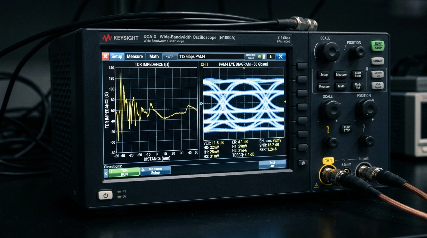
You are three weeks behind schedule. Your accelerator baseboard for an AI server just came back from assembly. The retimers lock sometimes. The 112G lanes train on one backplane slot, then collapse on the next. The compliance eye looks acceptable in simulation, but on the bench the margin evaporates. You open the scope capture and feel that familiar dread: vertical eye closure, bathtub curves sliding the wrong direction, random errors that refuse to reproduce cleanly. The board is not dead enough to diagnose fast, and not alive enough to ship. The worst kind of failure.
This is where signal integrity stops being an abstract checkbox and becomes a budget event.
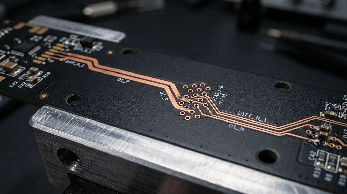
At 448 Gbps aggregate lane architectures and beyond, the harsh physics of the interconnect dominate everything. A via stub that looked harmless at yesterday's data rate becomes an insidious resonator. A breakout choice under a 0.4 mm pitch package adds just enough discontinuity to poison the channel. A differential pair that is "close enough" on geometry creates skew, mode conversion, and crosstalk that traditional workflows fail to predict in time. The market window does not wait. The board has failed. The re-spin conversation begins.
This article is a deep dive into how AI is changing high-speed PCB design in 2026, specifically for crosstalk, jitter, and PAM4/PAM8 signaling. The core shift is simple: instead of burning compute time on brute-force sweeps and late-stage Monte Carlo campaigns, modern teams are using AI predictive models trained on field-solver data, measurement libraries, and fabrication-aware stackup constraints to identify failure mechanisms before layout hardens. That is not hype. It is the new engineering baseline.
The Physics of Modern Channels: Why 2026 Is Different
A 2026 high-speed channel is no longer a copper trace plus a connector plus optimism. It is a distributed electromagnetic structure whose behavior is set by conductor roughness, dielectric loss tangent, launch geometry, return-path continuity, package escape topology, and process variability across fabrication and assembly.
For PAM4 and emerging PAM8 links, the signal levels are packed closer together than legacy NRZ systems. That means the eye is inherently more fragile. You are no longer deciding whether the receiver sees a 1 or a 0. You are protecting multiple amplitude levels with tighter voltage spacing and tighter timing margins, while also controlling insertion loss, return loss, skew, and common-mode conversion across the entire channel.
Three forces dominate most bring-up failures:
Crosstalk, where adjacent channels couple energy through mutual capacitance and inductance
Jitter, where transition timing uncertainty consumes horizontal eye opening
Channel discontinuities, where vias, breakouts, connectors, and package transitions create reflections and inter-symbol interference
That is why PCB layout design services for AI hardware, networking gear, storage systems, and accelerator modules now demand fabrication-aware SI strategy from the first placement pass.
Technical Deep Dive: The SI Math Behind Crosstalk
Crosstalk is the result of electric and magnetic field coupling between structures that should have been isolated enough, but were not. In coupled transmission lines, near-end crosstalk (NEXT) and far-end crosstalk (FEXT) depend on the balance between capacitive and inductive coupling, the edge rate, the coupled length, the dielectric environment, and whether the geometry is stripline, microstrip, broadside, or some hybrid transition through a breakout region.
At a simplified level:
Mutual capacitance (C_m) drives capacitive coupling
Mutual inductance (L_m) drives inductive coupling
Crosstalk voltage scales with edge rate (dV/dt) and coupled length
Differential pair imbalance converts differential energy into common mode, which then radiates, reflects, and corrupts adjacent structures
For a first-order view, capacitive crosstalk current is proportional to:
[ i_c = C_m \frac{dV}{dt} ]
and inductive crosstalk voltage is proportional to:
[ v_l = L_m \frac{di}{dt} ]
That looks harmless on paper. It is not. At modern edge rates, (\frac{dV}{dt}) and (\frac{di}{dt}) are enormous, so tiny geometry errors become measurable eye degradation.
For differential signaling, the more relevant question is not "is there crosstalk?" but "how much crosstalk converts into eye closure and BER degradation?" In practice, the engineer cares about:
aggressor-victim spacing
parallel run length
broadside coupling through adjacent layers
reference plane quality
return current continuity around anti-pads and split planes
pair-to-pair skew
via field density under BGAs and connectors
The old reflex was to run a rule-based spacing check, maybe a few 2D field solves, then launch a massive Monte Carlo campaign late in the cycle. That approach breaks down for dense AI boards. It is too slow, too fragmented, and too dependent on the exact scenarios you happened to simulate.
How AI Replaces Traditional Monte Carlo Workflows
Traditional Monte Carlo simulation perturbs geometry, material, and process variables across thousands of runs to estimate a statistical distribution of outcomes. It is rigorous, but computationally expensive and usually too late. By the time you see the distribution, placement is frozen, breakout topology is set, and the expensive mistakes are already baked in.
AI predictive modeling changes the sequence.
Instead of only running brute-force sweeps, modern workflows train surrogate models on:
2D and 3D field-solver outputs
measured TDR and VNA data from prior builds
fabricator process windows for etch, dielectric thickness, and plating variation
package and connector library data
stackup-dependent impedance and loss behavior
The model then predicts eye closure, crosstalk sensitivity, jitter contribution, and likely hotspot regions in near real time. You still validate critical paths with full-wave simulation. You still measure. But you do not wait until the end to discover what was predictable at placement time.
The payoff is speed and coverage. An AI model can evaluate far more geometry combinations than a manually curated Monte Carlo plan, especially for dense breakout regions and coupled lane bundles. It also highlights interaction effects that teams often miss, such as the combined penalty of glass-weave skew, roughness-induced loss, and asymmetrical reference transitions.
The Right Way
Train or use SI-aware surrogate models from fabrication-realistic data
Score candidate routes before finalizing topology
Focus full-wave simulation on the highest-risk structures
Continuously correlate model predictions with bench TDR, VNA, and BER data
The Wrong Way
Assume a spacing rule from older generations still applies
Run a limited Monte Carlo set after layout is effectively done
Treat breakout routing as a local problem instead of a channel problem
Ignore process variability until first articles fail compliance
Jitter in PAM4 and PAM8: The Horizontal Margin Crisis
If crosstalk eats your vertical eye opening, jitter destroys your timing margin. For PAM4, and even more so for PAM8 experimentation in advanced interconnect research, the horizontal budget is brutally tight. The receiver must decide not only whether a transition happened, but whether it happened at the correct time and at the correct level under channel distortion.
A useful decomposition is:
[ J_{total}(BER) = J_{RJ}(BER) + J_{DJ} ]
where:
(J_{RJ}) is random jitter, typically modeled with a Gaussian distribution and scaled to target BER
(J_{DJ}) is deterministic jitter, including duty-cycle distortion, periodic jitter, data-dependent jitter, and bounded uncorrelated effects
At the channel level, data-dependent jitter often comes from inter-symbol interference:
[ y(t) = x(t) * h(t) + n(t) ]
where (h(t)) is the channel impulse response. If (h(t)) has long tails from loss and reflections, prior symbols contaminate the current symbol decision. In PAM4, that means one bad transition can smear several adjacent symbol decisions. In PAM8, the situation gets even harsher because level spacing is narrower and equalization burden rises.
AI helps because jitter is rarely caused by one thing. It is the sum of channel loss, package effects, reference noise, PLL behavior, lane-to-lane coupling, and receiver equalization interaction. Classical analysis can decompose it, but it is slow and manually intensive. AI models can ingest waveform captures, TIE histograms, equalizer settings, and power rail noise signatures, then estimate which mechanisms dominate. That means the fix is targeted.
Sometimes the answer is route separation. Sometimes it is via backdrilling. Sometimes it is breakout symmetry under the ASIC. Sometimes it is a PDN problem masquerading as SI.
PAM4, PAM8, and the New Layout Penalties
PAM4 is already mainstream in leading-edge data center and networking links. PAM8 is not yet universal deployment territory, but in 2026 it is part of advanced planning discussions because aggregate throughput pressure is relentless. Either way, the channel demands are converging toward one conclusion: the PCB can no longer be treated as a passive afterthought.
For PAM4 and higher-order modulation, you must manage:
insertion loss slope across the Nyquist region
impedance discontinuities at every launch and transition
skew inside differential pairs and across lane groups
return loss from anti-pad and via geometry
crosstalk from tightly packed bundles
reference plane discontinuities that create mode conversion
That is why routing a 448 Gbps class system is not merely "faster Ethernet design." It is a multidisciplinary exercise across stackup engineering, package escape, connector strategy, and measurement correlation.
SLP and mSAP: Why Fabrication Technology Is Now an SI Variable
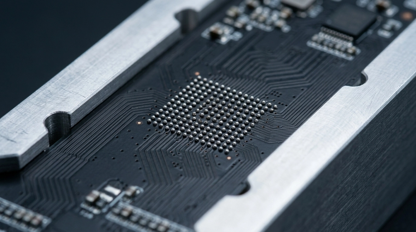
As package pitch shrinks and lane density rises, conventional subtractive PCB processes struggle to deliver the line width, spacing control, and breakout density needed without SI penalties. That is where substrate-like PCB (SLP) and mSAP enter the discussion.
SLP bridges the gap between conventional HDI boards and package-substrate-like routing density. It enables finer features, tighter registration, and cleaner breakout strategies for compact, high-I/O devices. For 0.4 mm pitch BGAs and advanced compute modules, SLP can dramatically reduce breakout congestion and shorten the ugly, discontinuity-heavy escape routes that destroy channel quality.
mSAP—modified semi-additive process—supports finer traces and spaces with better geometric control than traditional subtractive etching. That matters because geometry variation directly affects impedance and coupling. Better sidewall definition and tighter process control can improve repeatability across dense high-speed structures.
But these are not automatic wins. SLP and mSAP also introduce new constraints:
tighter fabrication capability matching
different cost structures
more careful DFM negotiation with the selected manufacturer
stackup and copper profile decisions that must be validated against real fab rules
The right engineering move is not "use the fanciest process." The right move is to choose the fabrication approach that gives the required electrical performance with manufacturable yield and acceptable cost. That is where a disciplined high-speed PCB design workflow matters.
Industry Application: AI Servers and Data Centers
The strongest pull for AI-driven SI methodology is coming from AI servers, accelerator cards, switch fabrics, retimer-heavy baseboards, and data center infrastructure. These systems combine exactly the conditions that punish sloppy design:
extremely high lane counts
long and heterogeneous channels
dense BGA escapes
aggressive power delivery transients
strict thermal and mechanical packaging limits
compressed validation schedules
In these environments, the old sequence of "layout, simulate a few channels, build, debug, re-spin" is economically unacceptable. A single board spin can delay qualification, consume lab time, block firmware teams, and defer revenue. That is why data center hardware teams are shifting to AI-assisted pre-layout and in-layout prediction.
A good AI-assisted SI workflow for server hardware does four things:
Ranks channel risk early. Before routing is complete, it identifies which links are likely to fail eye or BER targets.
Flags geometry sensitivity. It shows where spacing, anti-pad size, skew, or via topology have disproportionate impact.
Maps design choices to manufacturability. It uses fabrication-aware constraints instead of idealized geometry assumptions.
Improves lab correlation. It learns from TDR, VNA, and scope data so future boards converge faster.
For accelerator motherboards, switch cards, and smart NIC platforms, that is not a luxury. It is schedule protection.
Consultant Checklist: What to Audit Before You Commit the Layout
If you are evaluating internal work or external PCB layout design services, use this checklist before release:
Channel Architecture
Are the critical channels identified by data rate, modulation type, insertion loss budget, and BER target?
Are the longest and most discontinuity-heavy paths ranked by risk?
Are package, connector, and PCB portions modeled as one channel, not separate silos?
Stackup and Materials
Is the stackup selected for impedance control, loss, and reference integrity at the target Nyquist frequency?
Have roughness, resin content, and fabrication tolerances been included?
Are SLP or mSAP options justified by density and electrical need, not trend-following?
Breakout and Via Strategy
Is the 0.4 mm pitch BGA breakout optimized for return path continuity and minimal stubs?
Are microvias, backdrilling, or via-in-pad choices tied to actual SI benefit?
Are anti-pad and capture pad shapes tuned for launch quality?
Crosstalk Control
Are pair-to-pair spacing and broadside coupling analyzed with field-solver-backed data?
Are dense lane bundles screened for hotspot regions rather than checked by one global rule?
Has common-mode conversion risk been reviewed at asymmetrical transitions?
Jitter and Eye Margin
Is jitter budget allocated across transmitter, channel, clocking, and receiver equalization?
Has ISI been evaluated using realistic channel impulse response data?
Are power integrity and reference noise being treated as contributors to jitter?
AI Workflow Quality
Is the AI model trained or calibrated from real measurement and fabrication-aware simulation data?
Is there a correlation loop from prediction to TDR/VNA/BER measurement?
Are full-wave simulations still used on the highest-risk structures?
Manufacturing Readiness
Are fab rules validated against the target manufacturer's published capability?
Is there a DFM/DFT review before file release?
Are Gerbers, drill files, stackup notes, impedance tables, and assembly outputs internally consistent?
ROI Analysis: Why Predictive SI Beats Late Debug
The financial argument for AI-driven SI is straightforward. Traditional Monte Carlo-heavy flows often spend compute and engineering time late, when design freedom is lowest and fix cost is highest. AI predictive modeling moves insight earlier.
Here is the real ROI:
Cost Driver | Legacy Flow | AI-Predictive Flow |
|---|---|---|
Channel risk discovery | Late, after route maturity | Early, during placement and breakout planning |
Simulation efficiency | Heavy brute-force sweeps | Fast surrogate screening plus focused full-wave validation |
Lab debug time | Long, root cause unclear | Shorter, likely failure modes pre-ranked |
Re-spin risk | Higher | Lower |
Manufacturing alignment | Often idealized until handoff | Included earlier via fabrication-aware constraints |
Even one avoided re-spin can justify the method. But the bigger gain is engineering velocity. Your SI team spends less time hunting invisible interactions and more time solving ranked problems. Your hardware schedule stops bleeding days into exploratory debug. Your validation becomes more clinical, more traceable, and less dependent on heroic bench work.
For startups, that can preserve runway. For data center hardware teams, it can protect qualification windows and launch timing. For contract manufacturers and system integrators, it can prevent expensive blame-shifting after first articles fail.
The Right Way vs. The Wrong Way
Feature | The Wrong Way | The Right Way |
|---|---|---|
Crosstalk | Generic spacing rules copied from older boards | AI-ranked hotspot analysis tied to actual geometry and stackup |
Jitter | Measured late, decomposed manually | AI-assisted decomposition linked to channel and PDN behavior |
PAM4/PAM8 readiness | Assume equalization will save the link | Design the passive channel to preserve margin first |
Monte Carlo strategy | Huge late-stage brute-force campaigns | Predictive AI screening plus targeted signoff simulation |
SLP/mSAP usage | Selected for marketing appeal | Selected only when density and SI justify the process |
Validation | Scope screenshots without closed-loop learning | Bench correlation feeding future model accuracy |
FAQ
What is the biggest SI challenge at 448 Gbps in 2026?
Usually not one thing. It is the interaction of loss, crosstalk, reflections, skew, and jitter across package, PCB, and connector structures. The failure mode is systemic.
Is AI replacing electromagnetic simulation entirely?
No. AI is replacing a large amount of repetitive exploration and late-stage Monte Carlo work. Critical structures still need rigorous field solving and bench validation.
Why does PAM4 make PCB design harder than NRZ?
Because the eye has more levels and less margin between them. That makes amplitude noise, timing uncertainty, and ISI much more damaging.
Is PAM8 production-ready for every system?
No. PAM8 is part of advanced signaling conversations in 2026, but it comes with even tighter margin and equalization demands. Most teams should treat it as an emerging challenge, not a casual upgrade.
When should I consider SLP or mSAP?
When package pitch, breakout density, and impedance-control demands exceed what a conventional process can deliver cleanly. The decision should be driven by electrical and manufacturing analysis, not trend pressure.
Can AI help with crosstalk specifically?
Yes. AI models can rank aggressor-victim sensitivity, predict hotspot regions, and estimate eye impact from route geometry far faster than manual sweep workflows.
What measurements still matter on the bench?
TDR, VNA, eye diagrams, BER testing, and correlation of measured channel behavior to the design model. AI is only useful when grounded in reality.
Conclusion: From Dread to Design Control
High-speed failures feel catastrophic because they usually surface late, when budgets are stressed and options are narrow. But the underlying physics are not mysterious. Crosstalk, jitter, discontinuities, and process variation leave signatures. The opportunity in 2026 is that AI can now detect those signatures earlier and more systematically than traditional workflows built around delayed Monte Carlo campaigns.
That is the bridge between theory and production reality.
At Circuit Board Design, we approach high-speed PCB design with fabrication-aware constraints, disciplined SI analysis, DFM/DFT review, and measurement-minded layout execution. If your next platform involves 448 Gbps architectures, dense BGA escapes, SLP or mSAP decisions, or fragile PAM4 channels, the right workflow is not guesswork and not brute-force alone. It is predictive, validated, and engineered for manufacturable success.
Need expert support for signal integrity-critical hardware? Explore our PCB layout design services or contact us to discuss your next server, networking, or accelerator board.
Your channel budget is tight. Your methodology cannot be loose.


