
PCBSchemaGen: Automating Schematic Design with LLMs and Knowledge Graphs
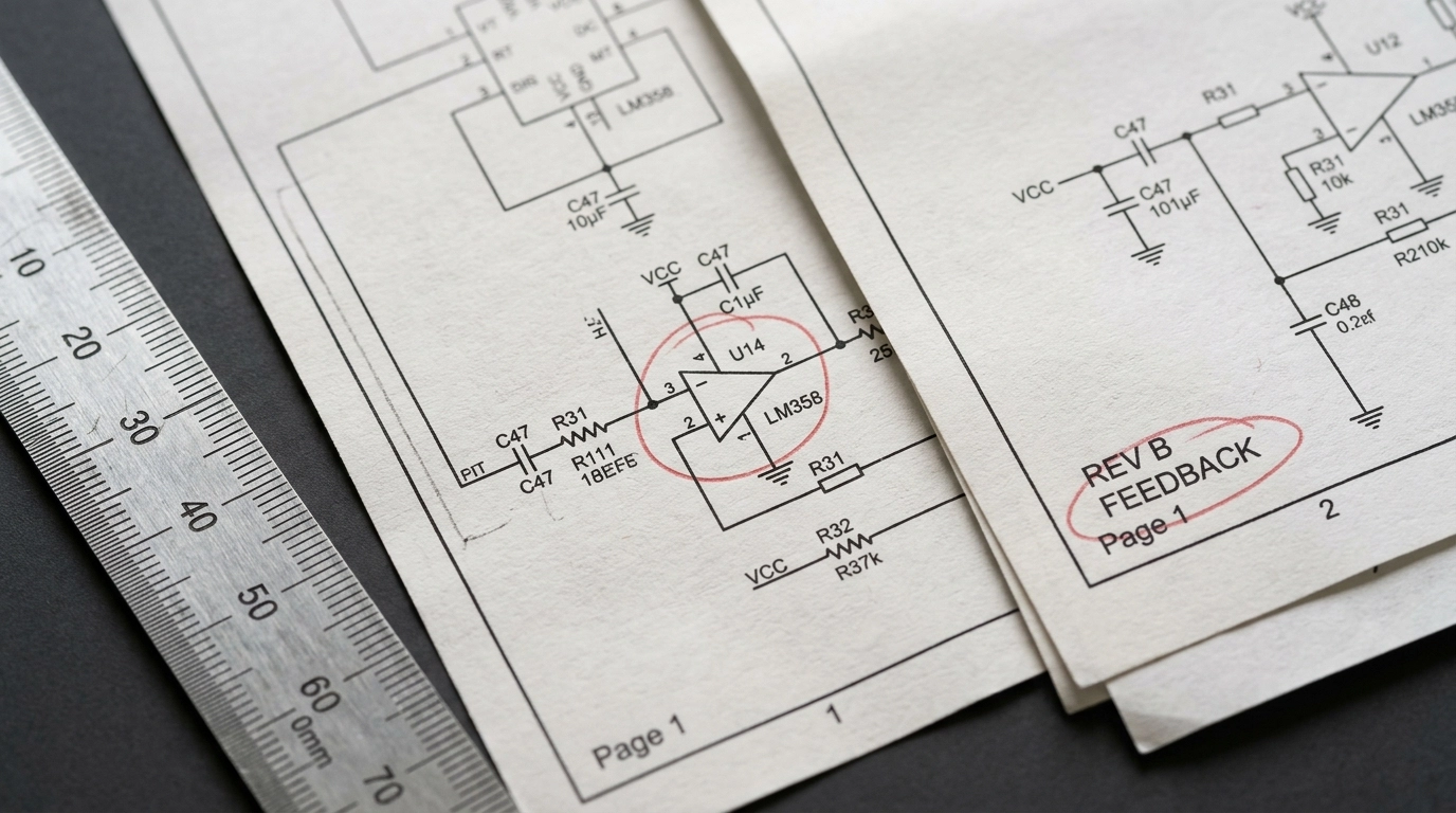
You are deep into a late-night design review, one tab open to a 300-page datasheet, another to Altium, another to KiCad, and a fourth to a distributor page that just marked your preferred regulator as “backordered.” The deadline is no longer theoretical. It is now. You’ve been manually mapping pins, power domains, pull-ups, boot straps, and protection parts for hours, and that cold dread starts to settle in. Did you miss a no-connect that is actually “reserved, tie low”? Did you copy the wrong reference design variant? Did the analog ground quietly merge with a dirty switching return three pages ago?
This is the kind of mistake that causes real heartburn. A tiny symbol-library inconsistency. One insidious net label typo. One polarity error buried inside a repeated channel. Then the prototype shows up, the board refuses to enumerate, your schedule evaporates, and what should have been a clean build becomes a forensic exercise in rework, bodge wires, and stakeholder damage control.
That failure feels emotional because it is emotional. But the root problem is not emotion. It is representation.
Modern electronics are not failing because engineers forgot Ohm’s law. They fail because the abstraction layer between component knowledge and schematic capture is still too manual. We ask humans to translate messy PDFs, vendor app notes, and tribal knowledge into a symbolic graph by hand, then act surprised when complexity wins. This is exactly where AI schematic generation becomes useful, provided it is grounded in physics, validated against rules, and never allowed to freestyle its way into production.
That is the promise of PCBSchemaGen: not “AI magic,” not a black box, and definitely not a robot that replaces engineering judgment. It is a structured pipeline that combines Large Language Models with machine-readable electronics knowledge so the first draft of a schematic can be generated, checked, corrected, and prepared for downstream PCB work much faster than traditional manual entry.
Technical Deep Dive: The Math Behind PCBSchemaGen
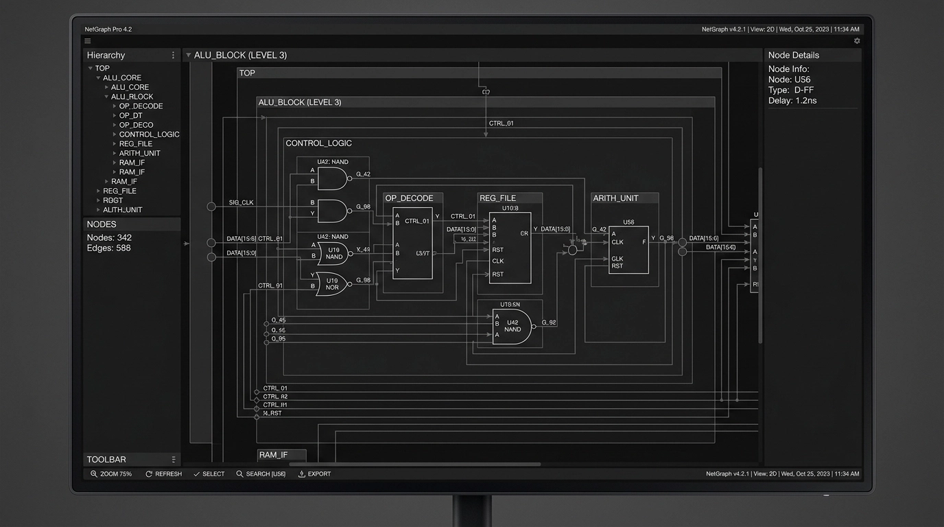
At a high level, PCBSchemaGen treats a schematic not as a picture but as a graph.
That sounds obvious, but it matters. A conventional EDA file displays symbols, pins, wires, ports, labels, and attributes. Underneath, though, the useful mathematical structure is a graph ( G = (V, E) ), where:
- ( V ) is a set of vertices representing symbols, pins, nets, ports, power rails, and sometimes functional blocks
- ( E ) is a set of edges representing valid electrical or logical relationships between them
For a simple resistor divider, that graph is small. For a modern embedded design with PMICs, RF front ends, USB-C, sensors, memory, and a wireless SoC, it becomes a dense constraint system. That density is where manual drafting starts to crack.
The Physics of the Semantic Gap
The “semantic gap” in EDA is the difference between what a tool can draw and what the design actually means.
A generic wire between two pins is just topology. It does not automatically encode whether that connection is:
- electrically valid
- functionally required
- conditionally allowed
- layout-sensitive
- safety-critical
- forbidden under IPC or manufacturer guidance
A pin named SDA is not merely text. It carries role semantics: open-drain behavior, a pull-up requirement, voltage domain constraints, bus-sharing rules, and expected adjacency to a companion SCL net. A switching regulator feedback node is not just a net label. It is a high-impedance analog sense node whose routing and component selection affect loop stability, noise, and emissions.
LLMs are good at pattern completion. Electronics demands constrained reasoning. So the only sane way to use an LLM in schematic capture is to cage it inside a formal structure.
The Math of Knowledge Graphs for Electronic Symbols
A Knowledge Graph for electronics is a typed graph in which entities and relationships are explicit.
Let:
- ( C ) = set of components
- ( P ) = set of pins
- ( N ) = set of nets
- ( A ) = set of attributes
- ( R ) = set of relationship types
Then the Knowledge Graph can be modeled as a heterogeneous graph:
[ G_k = (V_k, E_k, \tau_v, \tau_e) ]
Where:
- ( V_k = C \cup P \cup N \cup A )
- ( E_k \subseteq V_k \times V_k )
- ( \tau_v ) maps each node to a type such as component, pin, net, function, package, voltage-domain
- ( \tau_e ) maps each edge to a semantic relation such as
has_pin,requires_pullup,belongs_to_domain,must_connect_to,must_not_connect_to,decoupled_by, orreferences_footprint
This matters because symbols stop being dumb drawings and become machine-validated objects.
For example, a microcontroller node may have relationships like:
- MCU
has_pinPA9 - PA9
pin_functionUSART1_TX - PA9
supports_voltage_domainVDDIO - VDDIO
requires_decoupling100nF close-placement class - NRST
requires_pullup10k typical - USB_DP
must_pair_withUSB_DM - USB_DP
requires_impedance_class90-ohm differential downstream in layout stage
Now the system can reason about the schematic beyond mere syntax.
Symbol Embeddings and Similarity
Knowledge Graphs also let us compute useful similarity scores when vendor data is inconsistent. If symbol ( s_i ) and symbol ( s_j ) have neighborhoods ( \mathcal{N}(s_i) ) and ( \mathcal{N}(s_j) ), then representation-learning methods can embed them in a vector space:
[ f: V_k \rightarrow \mathbb{R}^d ]
Where semantically similar parts land near each other. That helps when reconciling alternate MPNs, different library naming conventions, or supplier substitutions.
A rough scoring function for candidate equivalence might combine:
- pin-count match
- functional role overlap
- package compatibility
- supply voltage compatibility
- interface support
- manufacturer notes or errata flags
[ Score(a,b) = w_1 S_{pins} + w_2 S_{func} + w_3 S_{pkg} + w_4 S_{volt} + w_5 S_{iface} ]
That is how you prevent the classic AI blunder of swapping “looks kind of similar” for “is electrically interchangeable.” In hardware, “close enough” is how budgets catch fire.
RAG for Part Selection: Retrieval Before Generation
If you let a model invent part numbers from memory, you are asking for pain.
Retrieval-Augmented Generation fixes this by separating knowledge access from language generation. Instead of prompting an LLM to “pick a 3.3 V regulator for an ESP32 board,” the system first retrieves candidate parts and design context from a trusted corpus:
- internal approved parts lists
- vetted symbol and footprint libraries
- datasheet excerpts
- application notes
- manufacturer reference designs
- stock and lifecycle metadata
- past project patterns
- rule decks for Altium or KiCad
Then the LLM operates only on retrieved evidence.
Formally, for a query ( q ), a retriever returns top-( k ) documents:
[ D_k = \operatorname{Retrieve}(q, \mathcal{D}, k) ]
The generator then produces an answer or schematic fragment conditioned on those documents:
[ y = \operatorname{Generate}(q, D_k) ]
In practice, the query is not just text. It is often a structured packet:
- target rails
- max current
- dropout budget
- noise tolerance
- input source
- thermal limits
- package constraints
- sourcing preferences
- compliance requirements
- allowed vendors
That makes part selection much less “chatbot” and much more engineering.
Ranking Candidate Parts
A useful candidate-part ranking score often looks like a weighted objective function:
[ J(p) = \alpha_1 \cdot Fit_{electrical}(p) + \alpha_2 \cdot Fit_{availability}(p) + \alpha_3 \cdot Fit_{cost}(p) + \alpha_4 \cdot Fit_{footprint}(p) + \alpha_5 \cdot Fit_{compliance}(p) - \alpha_6 \cdot Risk(p) ]
Where:
- ( Fit_{electrical} ) checks voltage, current, tolerance, speed, thermal headroom, and interface compatibility
- ( Fit_{availability} ) captures stock, lead time, and lifecycle status
- ( Fit_{footprint} ) checks package and assembly feasibility
- ( Fit_{compliance} ) checks RoHS, REACH, UL, or other project constraints
- ( Risk ) penalizes parts with missing models, poor sourcing, known errata, or questionable substitutes
This is why AI schematic generation is most effective when paired with disciplined procurement-aware retrieval. Otherwise, you get a beautiful schematic around a part nobody can buy.
How LLM-Driven Schematic Generation Actually Works
Here is the practical workflow.
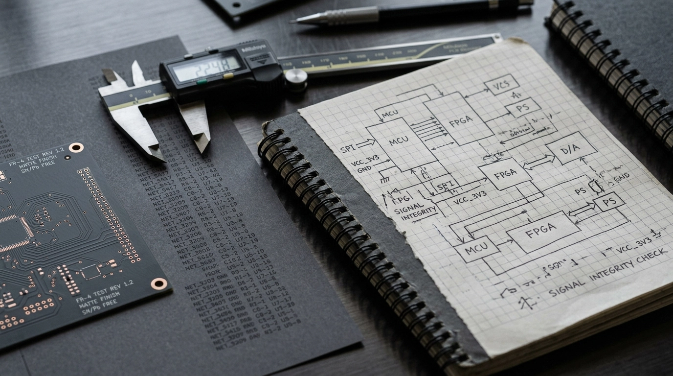
Specification ingestion
The input may be a product requirement document, a block diagram, an email, or a terse engineer note like: “Battery-powered IoT sensor node, ESP32-S3, LTE fallback, USB-C power, Li-ion charger, 3.3 V digital, 1.8 V sensor rail, low sleep current, FCC/CE target.”Intent parsing
The LLM extracts blocks, rails, interfaces, likely protection needs, clocks, programming headers, and mandatory support circuits.Retrieval stage
The system queries internal libraries and structured references for approved symbols, footprints, known-good subcircuits, and datasheet constraints.Graph assembly
The design is instantiated as a typed graph. Functional blocks become subgraphs. Candidate connections are proposed with constraints attached.Rule validation
Electrical rule checks, domain compatibility checks, graph-pattern checks, and template conformity checks run before the schematic is emitted.Code or EDA output generation
The netlist or intermediate representation can be rendered into SKiDL, then exported to KiCad, or mapped into library-backed schematic constructs for Altium workflows.Human review
Senior engineers review what matters most: power tree logic, corner cases, signal-integrity-sensitive interfaces, safety spacing intent, and manufacturability implications.
This is the correct human-in-the-loop model. Fast where automation is strong. Conservative where reality is harsh.
The Mechanics of Constraint Checking
A good system does more than match keywords. It checks topology.
Suppose a known-good buck converter pattern is represented as a reference subgraph ( G_r ), and the generated design contains a candidate subgraph ( G_c ). We can test whether the generated circuit structurally matches the required pattern using subgraph isomorphism.
[ G_r \cong G_c ]
That means the required relationships exist, even if reference designators or physical coordinates differ.
Typical checks include:
- regulator feedback divider present and connected correctly
- bootstrap capacitor exists between required nodes
- I2C bus has pull-ups in the correct voltage domain
- differential pairs are properly paired in the logical netlist
- reset and boot mode pins are not left floating
- decoupling capacitors exist per rail and quantity class
- crystal load capacitors and bias network follow vendor guidance
- USB-C CC logic and protection devices are present
This is where automation becomes clinically useful. It does not get bored. It does not get sleepy. It does not start trusting a bad app note because it is 1:30 a.m.
Maintaining IPC Standards While Automating
This is the part people often skip, and it is the part that separates a demo from a production workflow.
At Circuit Board Design, any automated schematic flow must still support the reality of downstream PCB implementation. We design to IPC-2221 principles and validate against real fabrication and assembly constraints before release. That means the schematic cannot be generated in a vacuum.
The automation layer needs to preserve:
- clear reference designator discipline
- coherent net naming
- hierarchical sheet structure
- test point strategy where appropriate
- proper power-ground partitioning intent
- component metadata for BOM generation
- package linkage to verified footprints
- design notes that survive handoff into PCB layout and manufacturing
In other words, PCB design services do not get easier just because a model can draft symbols quickly. If anything, the need for rigorous structure increases.
The Right Way vs. The Wrong Way
The Wrong Way: ask an LLM to produce a complete schematic from raw prompt text, trust the answer, and throw it into layout.
That is not innovation. That is accelerated failure.
The Right Way: use the LLM as a front-end parser and orchestration layer over curated libraries, Knowledge Graph constraints, retrieval pipelines, ERC rule decks, and human review.
The difference is huge.
| Feature | Traditional Manual Design | LLM + Knowledge Graph Workflow |
|---|---|---|
| Primary Input | PDF datasheets, app notes, manual entry | Natural language specs + structured retrieval |
| Symbol Logic | Human memory and checklists | Typed graph with semantic constraints |
| Part Selection | Manual search across vendors | RAG-ranked candidates with filters |
| Validation | Human review + standard ERC | ERC + topology checks + domain rules |
| EDA Output | Manual drafting in Altium or KiCad | Assisted generation into review-ready schematics |
| Best Use | Simple or legacy designs | Repetitive, modular, and library-rich systems |
Industry Application: IoT and Consumer Electronics
The sweet spot for PCBSchemaGen is not “every possible board ever.” It shines where architectures repeat, constraints are known, and schedule pressure is intense.
IoT Devices
IoT designs are perfect candidates because they usually combine recurring blocks:
- microcontroller or wireless SoC
- sensors over I2C, SPI, UART, or ADC
- battery charging and power-path management
- low-dropout regulators and buck converters
- USB or pogo-pin programming interface
- ESD and surge protection
- antennas, matching, or module keep-out constraints
These blocks are repetitive enough for automation but still complex enough that manual errors are common. An LLM-driven workflow can rapidly instantiate support circuitry, retrieve approved parts, and build a draft schematic for engineering review. That speeds the path from dev kit to custom hardware, which is exactly where many startups need outside PCB design services.
Consumer Electronics
Consumer products add another layer of difficulty: cost pressure.
In these projects, the value of AI-assisted schematic capture is not just speed. It is consistency across variants. The same platform may spawn:
- a Bluetooth-only version
- a Wi-Fi + LTE version
- a premium model with extra sensors
- a low-cost SKU with fewer interfaces
A Knowledge Graph-backed generation flow makes it easier to reuse valid subcircuits, maintain variant control, and avoid subtle divergence between product branches. That helps when you are trying to hit a price target without quietly breaking EMC behavior, low-power performance, or assembly assumptions.
Consultant Checklist: What to Ask Before You Trust AI Schematic Generation
If you are evaluating a consultant, an internal workflow, or a tool claiming “AI-generated electronics,” ask these questions.
1. Is the system grounded in real component data?
If the answer is “it uses a powerful model,” keep walking. You need vetted symbols, footprints, datasheets, and library governance.
2. Does it use retrieval for part selection?
A serious workflow should use RAG or an equivalent retrieval layer to pull current, approved, project-specific part data before generation.
3. How are pin roles and prohibited connections represented?
Ask whether the system has typed pin semantics, voltage domain awareness, and must-connect / must-not-connect rules.
4. Can it output clean files for Altium or KiCad?
A fancy demo is useless if it dies before deliverables. Real projects need source files, PDFs, BOMs, and manufacturing-ready continuity into layout.
5. What validation happens before handoff?
Minimum acceptable answers include ERC, topology checks, library validation, and human engineering review.
6. How does it maintain IPC-aware design structure?
The schematic should support downstream compliance with IPC-2221, DFM review, testability, and assembly clarity.
7. Is it useful on your class of product?
The right consultant will tell you where automation fits and where it does not. High-speed DDR, isolated medical power, and mixed-signal precision analog still need very deliberate expert oversight.
ROI Analysis: Where the Business Case Actually Comes From
AI in hardware is often pitched like a magic productivity wand. The real ROI is more boring and more powerful.
It comes from reducing expensive, avoidable engineering friction.
Time Savings
Drafting repeated support circuitry manually is costly senior-engineer time. If the first-pass schematic skeleton is generated in hours instead of days, teams can spend that saved time on the work that actually differentiates the product: architecture, risk reduction, testing, firmware integration, and layout strategy.
Error Reduction
Manual transcription from datasheets is one of the most boring and dangerous tasks in electronics. That combination is lethal. A retrieval-backed, rule-validated flow reduces copy-paste mistakes, net naming inconsistency, and omitted support components.
Variant Reuse
Once valid subgraphs exist for common blocks, product-line expansion gets less painful. That directly affects startup timelines and consumer electronics margins.
Better Outsourcing Economics
For teams using external PCB design services, better input structure means fewer back-and-forth loops. A consultant can move from ambiguity to implementation faster when the generation pipeline produces a disciplined starting point.
A simple ROI model might look like this:
[ ROI = \frac{(T_s \cdot C_e) + C_r + C_v - C_i}{C_i} ]
Where:
- ( T_s ) = engineering hours saved
- ( C_e ) = cost per engineering hour
- ( C_r ) = avoided respin cost
- ( C_v ) = value of faster schedule or earlier revenue
- ( C_i ) = cost of implementing the workflow
The hidden monster in that equation is respin cost. One avoided board revision often pays for a lot of process improvement. Not glamorous. Very real.
FAQ
What is PCBSchemaGen?
PCBSchemaGen is a workflow for automated or assisted schematic capture that combines LLMs, Knowledge Graphs, retrieval pipelines, and validation rules to generate draft schematics from engineering intent.
Is AI schematic generation ready to replace hardware engineers?
No. It is best viewed as an acceleration layer for repetitive, structured tasks. Human review remains essential for architecture, compliance, analog behavior, high-speed interfaces, safety, and manufacturability.
Does this work with Altium and KiCad?
Yes, that is the practical goal. Automation is only useful if it can feed real engineering tools like Altium and KiCad with library-controlled outputs.
How does RAG help with part selection?
RAG retrieves trusted project-relevant data before generation. That means candidate parts are chosen from approved sources and evaluated using real constraints instead of model memory.
Are Knowledge Graphs overkill for electronics?
Not if you care about correctness. Symbol semantics, pin roles, voltage domains, and support-circuit requirements are relational by nature. Graphs are a natural fit.
Can this maintain IPC standards?
It can support them, yes, if the workflow is tied to disciplined libraries, constraint rules, ERC checks, and downstream review processes aligned with standards like IPC-2221.
From Idea to Reality: A Seamless Bridge
We’ve all seen the common reflex: skepticism, usually earned. Plenty of “AI hardware” demos collapse the moment they meet a real datasheet, a real BOM constraint, or a real compliance target. Fair enough. The field has produced its share of polished nonsense.
But the useful version of this story is much more grounded. When AI schematic generation is constrained by Knowledge Graphs, backed by RAG, and reviewed by experienced engineers, it becomes a practical accelerator for product teams that need reliable momentum. That is especially valuable when moving from concept to manufacturing-ready design data without adding months of manual library work.
At Circuit Board Design, we use automation where it genuinely helps and engineering discipline where it absolutely matters. That means support for schematic capture, library-backed implementation in Altium and KiCad, DFM-aware thinking, and a workflow built around manufacturable results, not AI theater.
Conclusion: Engineering with Confidence
The era of purely manual schematic entry is fading, not because engineers are becoming less capable, but because systems are becoming too interconnected, too variant-heavy, and too schedule-sensitive to justify brute-force drafting forever.
PCBSchemaGen is compelling because it bridges intent and implementation. It lets the machine handle the repetitive structure while humans handle judgment, edge cases, tradeoffs, and reality. That is the right division of labor.
If your team needs PCB design services that combine modern automation with actual engineering restraint, we can help. We support startups, product teams, and hardware groups that need faster schematic capture, cleaner handoff into layout, and confidence that the design logic still holds up under scrutiny.
The nightmare version of this story is familiar: missed nets, bad part choices, late-stage rework, blown budgets. The better version is quieter. Structured inputs. Verified outputs. Seamless handoff. Fewer surprises.
That is the whole point. Contact us today to discuss your next Altium, KiCad, or AI-assisted hardware design project.


