
Why You Need a PCB Design Consultant for 448 Gbps Signaling and Chiplet Integration in 2026
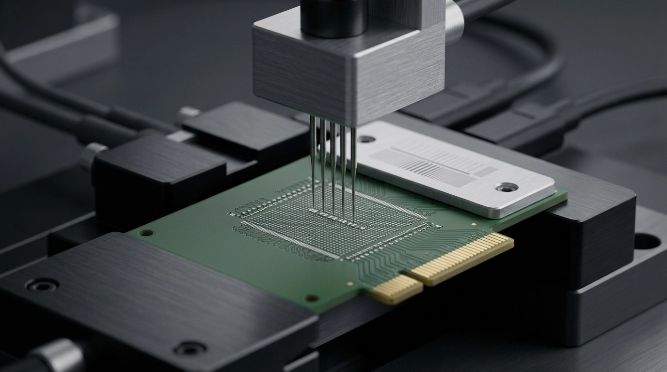
You are standing in the testing lab, the hum of the cooling fans sounding like a low-frequency funeral dirge. You’ve just spent six figures and four months on a high-density prototype. The power rails are stable. The firmware is flashed. But as you trigger the oscilloscope for the first 448 Gbps link test, the eye diagram doesn’t just look bad: it looks like a flatline.
There is no signal. Only a chaotic, metallurgical soup of jitter and thermal noise.
The dread sets in. Your market launch window evaporates. The investor demo is in three days, and your high-speed pathways have effectively become monolithic antennas radiating expensive heat into the chassis. This is the insidious reality of modern hardware engineering: at 448 Gbps, the copper on your board isn't just a conductor anymore. It’s a high-frequency electromagnetic waveguide that obeys no "rule of thumb" you’ve ever learned. The tombstone is set, and the board has failed.
Bridging the gap between a theoretical schematic and the harsh physical reality of 2026-era signaling requires more than just a layout tool; it requires a specialized PCB design consultant who understands that the physics has changed.
The Physics: Why 448 Gbps is a Different Beast
In the "old days": meaning 2024: we dealt with 112 Gbps or even 224 Gbps PAM4 signaling. You could still rely on traditional via structures and standard low-loss laminates if you were meticulous. In 2026, the jump to 448 Gbps (OIF-CEI-448G) has rendered traditional PCB layout methodologies obsolete.
At these frequencies, the skin effect is so aggressive that the signal travels only on the outermost molecular layer of the copper. Any surface roughness in the foil creates massive resistive losses. But the real killer? The vias. A standard through-hole via at 448 Gbps acts as a massive capacitive parasitic, reflecting the signal back to the source before it even reaches the first connector.
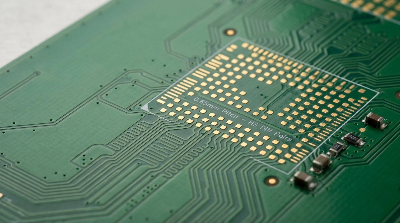
To survive this, a PCB design consultant must implement substrate-like PCB (SLP) construction and ultra-HDI (uHDI) techniques. We are moving toward package ballouts smaller than 0.65 mm pitch, where the "escape" from the BGA is a work of microscopic art. If your consultant isn't talking about modulation budgets, insertion loss slope, crosstalk density, return-loss targets, and quasi-TEM bandwidth, your design is already walking toward the cliff.
The Physics Behind 448 Gbps Signaling
At 448 Gbps, the failure mechanism is rarely one dramatic mistake. It is usually the aggregate cruelty of many small ones. Copper roughness. Resin loss tangent. Stub resonance. Connector discontinuity. Reference plane perforation. The board does not fail because one trace was "bad." It fails because the entire channel quietly exceeded its loss and noise budget.
That is why a serious PCB design consultant stops thinking in traces and starts thinking in channels. For 448 Gbps-class links, every segment matters: package escape, breakout, via field, connector launch, cable or backplane transition, and power integrity coupling into the channel. A few tenths of a dB in the wrong place can consume precious equalization margin. Then the eye collapses. Fast.
The harsh reality is that skin effect and dielectric loss are only the opening act. At these data rates, copper foil profile becomes economically significant because the signal current is concentrated near the conductor surface. Rough copper increases effective path length and loss. Backdrilling becomes mandatory in many architectures because via stubs create resonant structures that chew into the Nyquist region. Return current continuity is no longer a best practice; it is survival. If your differential pair crosses split planes, antipads are oversized without modeling, or stitching vias are treated as decoration, your EMI and signal integrity problems become welded together.
A capable PCB design consultant also knows that 448 Gbps is not merely "faster 112G." The design methodology changes. You validate stackup options against actual fabricator capabilities. You control glass weave effects where practical. You specify copper treatment, resin content, foil type, and drill strategy with manufacturing in the room, not after the fact. This is the difference between theoretical performance and a link that passes on the bench.
The Materials Science: SLP, mSAP, and Why the Copper Itself Matters
This is where the conversation gets expensive, and where amateurs usually flinch.
SLP and mSAP are not buzzwords to sprinkle into a slide deck. They are process-level decisions that fundamentally change routing density, impedance consistency, and insertion loss behavior. Substrate-like PCB technology enables finer lines, tighter spaces, smaller vias, and denser BGA escape patterns that traditional subtractive etch processes struggle to deliver cleanly. Modified semi-additive process (mSAP) pushes conductor definition further by building copper where needed instead of etching away large areas from thick foil. The result is straighter sidewalls, finer geometries, and more predictable conductor dimensions.
Why does that matter? Because at extreme data rates, conductor geometry error becomes electrical error. If your trace width varies, your impedance varies. If your etch profile is sloppy, current crowding changes. If your dielectric thickness meanders, so does your channel response. You do not just get a manufacturing defect. You get jitter, mode conversion, and compliance pain.
The right way is to choose material and process as a unified system:
SLP when the package escape density and via strategy demand ultra-fine geometry.
mSAP when conductor precision and line/space control must support extremely tight impedance windows.
Low-loss laminates when dielectric attenuation and thermal stability matter more than raw laminate cost.
HVLP or smoother copper options when conductor loss is consuming your budget.
Sequential lamination and laser microvias when escape routing and layer transitions must remain compact and electrically disciplined.
The wrong way is cheaper on the quote sheet and catastrophic in bring-up. You save a few thousand dollars in fabrication assumptions and then spend ten times more debugging reflections, skew, and unpredictable yield.
The Mechanics: Chiplet Integration and STCO
The era of the monolithic SoC is over. Everything in 2026 is a chiplet. Whether you are building an ADAS radar processing unit or a next-gen AI accelerator, you are likely dealing with heterogeneous integration.
This is where System-Technology Co-Optimization (STCO) becomes the primary differentiator between success and catastrophic failure.
STCO isn't just about placing chips close together. It’s about a holistic design approach where the package, the substrate, and the PCB are designed as a single, unified electrical entity. As your PCB design consultant, we don't just "receive" a footprint; we participate in the co-optimization of the vertical interconnects. We analyze thermal dissipation across the chiplet boundaries and ensure that the power delivery network (PDN) can handle the transient currents required by multi-die architectures without inducing brownouts or ground bounce.
STCO in the Real World: Package, Substrate, Board, and Thermal Stack as One System
In practice, STCO means accepting a simple truth: the package engineer, SI engineer, thermal engineer, and PCB layout specialist are all working on the same problem whether they admit it or not. A chiplet-based design can fail even when each domain appears "locally optimized." That is the trap. The package may look elegant, the substrate may pass its own checks, and the board may be manufacturable. Yet the assembled system can still suffer from rail collapse, simultaneous switching noise, differential skew, warpage, or thermal gradients that wreck reliability.
A seasoned PCB design consultant bridges that gap early. We review chiplet bump maps, breakout topology, reference plane transitions, decoupling hierarchy, and power entry architecture before layout momentum makes the wrong decisions feel inevitable. We align package escape assumptions with actual board stackup options. We look at where current returns, where heat spreads, where vias choke airflow, and where mechanical constraints force ugly compromises.
For chiplet programs, the PDN discussion becomes especially brutal. Fast edge rates and clustered compute die create sharp transient loads. If the package inductance, board cavity design, and decap placement strategy are not considered together, the supply rails sag exactly when the workload spikes. That means intermittent failures, corrupted high-speed training behavior, and weeks of lab time chasing a problem that only appears under certain vectors or thermal conditions. Insidious. Expensive. Common.
The right STCO workflow treats these as first-order design inputs:
Bump-to-ball escape topology and layer assignment
Package-to-board transition loss and reference continuity
PDN impedance targets across frequency bands
Thermal spreading through substrate, board copper, and enclosure
Mechanical warpage risk from dense fine-pitch regions and asymmetric copper
DFM constraints that preserve, rather than sabotage, the electrical model
That is why a genuine PCB design consultant is valuable in chiplet programs. Not because they can push polygons around faster, but because they understand that package, substrate, PCB, and manufacturing are one coupled electromechanical problem.
The Chemistry: 3D-Printed EMI Mitigation and Microwave Holography
The higher the frequency, the more "leaky" the board becomes. Traditional metal shielding cans are often too bulky, too heavy, or simply ineffective against the complex interference patterns of 448 Gbps signals.
At Circuit Board Design, we specialize in a niche but essential expertise: 3D-printed EMI mitigation.
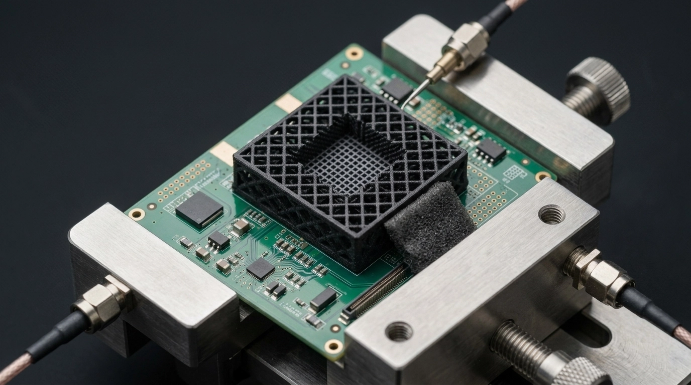
Instead of generic shielding, we utilize microwave holography to map the precise electromagnetic emissions of your board in a virtual environment. We then design and 3D-print custom, carbon-loaded absorbers that are tuned to the exact harmonic frequencies of your design. These aren't just covers; they are mathematically optimized structures that "swallow" interference.
This level of precision is reinforced by our IPC CID+ certification and disciplined traceability systems. We don't guess where the noise is coming from; we document the design intent, validate the implementation path, and then kill it with material science.
The Mechanics of Microwave Holography for EMI Debug
Microwave holography sounds exotic, but the engineering logic is practical: you reconstruct the near-field radiation behavior of a system with enough spatial fidelity to see where energy is escaping, coupling, and re-radiating. That matters because EMI problems on high-speed boards are rarely caused by a single obvious radiator. They emerge from current loops, slot antennas, connector launches, seam leakage, imperfect return paths, and resonant cavities in enclosures or shields.
The wrong way to solve EMI is with desperation hardware. Add a metal can. Add ferrites. Add tape. Add absorber foam. Hope the chamber result improves. Sometimes it does. Often it just moves the problem.
The right way is diagnostic first, countermeasure second. With microwave holography, you identify hot regions and understand whether the dominant issue is common-mode conversion, cavity resonance, edge radiation, cable excitation, or enclosure leakage. Then you tailor the mitigation strategy:
geometry changes that reduce loop area
stitching via fences that actually terminate field spread
shield segmentation based on field distribution
absorber placement only where it provides measurable attenuation
selective use of conductive or carbon-loaded printed structures to suppress the relevant modes
For dense products, especially those mixing RF, compute, motor control, or fast serial links, this approach can be the difference between a one-pass compliance story and a soul-crushing cycle of chamber retests.
Industry Deep Dive: Medical Devices
Medical electronics create a uniquely unforgiving intersection of precision measurement, patient safety, and regulatory scrutiny. In a medical monitoring device, the nightmare is not just a failed boot or a garbled data stream. It is common-mode noise coupling into an analog front end, leakage current concerns, false readings, or a radiated emissions issue that stalls certification under IEC 60601. The ramifications are clinical, legal, and reputational.
A PCB design consultant working in medical hardware has to design for more than speed. Isolation barriers, creepage and clearance, low-noise grounding, electrode interface protection, and coexistence between sensitive analog channels and digital subsystems all matter. If you are also incorporating wireless links, high-speed memory, or chiplet-based compute, the layout becomes a balancing act between patient safety and signal integrity.
The right way in medical design is disciplined partitioning. Quiet analog zones. Controlled return paths. Isolation components placed with intent rather than symbolism. Filter structures that are modeled, not copied from an eval board. Materials selected not just for loss performance, but for reliability through sterilization, cleaning, thermal cycling, and long service intervals. A consultant who understands both PCB design services and compliance realities can dramatically reduce the risk of late-stage redesign.
Industry Deep Dive: Aerospace & Defense
In aerospace, the board is not merely carrying data. It is surviving vibration, thermal shock, altitude, moisture excursions, and long mission profiles while preserving deterministic behavior. A 448 Gbps channel that "mostly works" in the lab is worthless if connector fretting, stackup drift, or enclosure-mode coupling destroys margin in the field. That is where the heartburn begins.
For avionics, payload electronics, or ruggedized edge compute, a PCB design consultant must consider signal integrity and mechanical integrity together. Backdrilled vias, rigid-flex transitions, retention of reference planes across connectors, and component anchoring strategy all matter. So does documentation. Aerospace teams often need disciplined traceability, controlled revision practices, and design rationale that survives audits and cross-functional review.
The wrong way is to optimize for bench aesthetics and ignore the operational envelope. The right way is to validate routing strategy, stackup, connector selection, mounting constraints, and environmental assumptions as one system aligned with MIL-STD-style realities. That is how you avoid field failures that cost more than the original NRE ever did.
Industry Deep Dive: Automotive
Automotive electronics are a special kind of brutal because they combine cost pressure with a hostile electrical environment. You are dealing with load dumps, cold crank, switching noise, thermal cycling, moisture, vibration, and increasingly dense compute for ADAS, infotainment, battery management, and zonal architectures. A board that behaves beautifully at room temperature can become erratic after enough thermal and mechanical stress. Then the warranty math starts bleeding.
In automotive programs, a PCB design consultant must think about DFM/DFT review, manufacturability at scale, test access, derating, EMC robustness, and standards-driven discipline from day one. For radar, camera processing, battery management systems, or high-speed in-vehicle networking, layout choices influence not just performance but line yield and long-term reliability. One sloppy return path or one marginal connector launch can create a compliance problem that ripples into schedule slip, requalification, and supplier friction.
The right way is to design with the production line and vehicle environment already in mind. Thermal paths must be credible. Power integrity must survive transients. High-speed interfaces must preserve margin across process spread and aging. This is where a specialized PCB design consultant earns their keep.
The Right Way vs. The Wrong Way
When hiring a PCB design consultant, you are choosing between two paths:
The Wrong Way: Treating the PCB as a "commodity" or a "drawing task." Handing a complex 448 Gbps design to a generalist who relies on auto-routers and generic manufacturing rules. The result? Manual rework, blown budgets, and a board that fails testing and validation.
The Right Way: Engaging an IPC CID+ certified expert who treats the PCB as the most critical component in the system. We provide a meticulous DFM/DFT review that validates every trace against real-world fabrication rules from partners like MacroFab and PCBWay before a single dollar is spent on manufacturing.
Consultant Checklist: What to Demand Before You Hand Over a High-Speed Project
If you are evaluating a PCB design consultant, use this checklist before the first kickoff call. If the answers are vague, evasive, or purely tool-centric, that is your warning.
1) High-Speed Channel Competence
Can they discuss loss budget, return loss, insertion loss, crosstalk, skew, and via resonance without hand-waving?
Do they understand how package escape, connector launch, and PCB stackup interact?
Can they explain when backdrilling, microvias, or alternative launch geometries are required?
2) Materials and Fabrication Literacy
Do they know when SLP or mSAP is justified?
Can they recommend laminate families based on loss, thermal behavior, and fab availability?
Do they validate designs against actual fabricator rules instead of generic EDA defaults?
3) STCO and Multi-Domain Thinking
Have they worked with advanced packages, chiplets, fine-pitch BGAs, or interposer-like escape constraints?
Can they coordinate package, thermal, PDN, mechanical, and PCB tradeoffs?
Do they recognize that a footprint is not a design strategy?
4) EMI / EMC Debug Methodology
Do they diagnose field problems systematically, or just add shield cans and ferrites?
Can they explain common-mode conversion, return path discontinuities, and enclosure coupling?
Are they comfortable with advanced mitigation workflows such as microwave holography-informed shielding concepts?
5) Compliance and Industry Context
Have they designed for medical, aerospace, automotive, industrial, or RF-heavy environments?
Can they align layout decisions with IEC 60601, MIL-STD-810, AEC-Q100, ISO 26262, FCC, or CE realities where relevant?
Do they understand test strategy, documentation, and traceability requirements?
6) Deliverables and Ownership
Will you receive Gerbers, NC drill, BOM, pick-and-place, assembly drawings, schematic PDFs, and native source files?
Is revision control disciplined?
Is the design manufacturing-ready, or are you buying a beautiful problem someone else must finish?
A real PCB design consultant should welcome this checklist. The wrong one will resent it.
The True Cost of "Good Enough"
In the hardware world, "good enough" is a psychological reflex that leads to ruin. A single signal integrity error in a 448 Gbps pathway can cost $50,000 in scrapped boards and months of lost market share. The heartburn of a failed bring-up is a rite of passage no founder should have to endure twice.
Working with an expert consultant isn't just an "expense": it is the essential bridge between a conceptual schematic and a production-ready product. We’ve completed over 500+ designs, ranging from avionics data recorders to medical monitoring devices, all adhering to the most stringent standards like IEC 60601 and MIL-STD-810.
Economic ROI: Why a PCB Design Consultant Is Usually Cheaper Than Failure
This is the part many teams avoid until the budget is already on fire.
A specialized PCB design consultant may look like a premium line item in early planning. But that view collapses the moment you model the cost of one failed prototype cycle in a high-speed or regulated product. The direct costs are obvious: fabrication, assembly, expedited components, lab time, compliance pre-scan fees, engineer time, and shipping. The indirect costs are worse: delayed demos, deferred revenue, missed customer commitments, investor anxiety, and opportunity cost for the engineering team now trapped in rework.
A realistic ROI model often looks like this:
Prototype fabrication and assembly for an advanced board: substantial
Expedite fees for constrained components and fast-turn manufacturing: painful
SI/EMI debug time across EE, firmware, and test teams: very painful
Compliance retest or chamber rebooking: brutal
Schedule slip on a funded product milestone: potentially catastrophic
Even conservative programs can lose tens of thousands of dollars on one bad turn. More complex programs can lose far more once system integration delays are included. By contrast, hiring a strong PCB design consultant usually shifts spending from reactive chaos to proactive engineering. Better stackup planning. Better escape routing. Better DFM. Better test access. Better documentation. Better first-pass outcomes.
A Simple ROI Thought Experiment
Assume your team spends:
$18,000 on fabrication, assembly, and logistics for a dense prototype run
$12,000 in internal engineering time for debug and rework coordination
$8,000 in schedule impact tied to delayed testing, partner dependencies, or missed demos
$7,000 in compliance pre-scan repeats or additional chamber-related effort
That is a $45,000 penalty for a single avoidable failure cycle, and it does not include morale loss or delayed revenue. If an experienced PCB design consultant reduces even one such respin, the engagement often pays for itself immediately. If the consultant also improves manufacturability, testability, and documentation quality, the ROI compounds through every later build.
For startups, this can preserve runway. For product companies, it protects launch timing. For engineering managers, it protects team focus. The return is not abstract. It is cash, schedule, and credibility.
Conclusion: From Nightmare to Seamless Production
The "nightmare" of the failing test bench doesn't have to be your reality. By integrating high-level expertise in 448 Gbps signaling, advanced materials such as SLP and mSAP, chiplet-aware STCO, and targeted EMI workflows informed by microwave holography, you can move from prototype to production with absolute confidence.
At Circuit Board Design, led by founder Niloy Mondal, we don't just layout boards; we engineer success. Whether you are a startup transitioning from a dev kit to a custom PCB or a massive R&D department needing burst capacity for a high-speed project, we are your dedicated partners in electronics engineering.
If you need a PCB design consultant who understands the physics, the manufacturing, and the business stakes, we are built for exactly that gap. Don't let your 2026 roadmap be derailed by 2024 design thinking. Contact us today for a quote within 48 hours, and let’s build something that actually works: the first time.
Frequently Asked Questions
How fast can a PCB design consultant typically turn around a project?
For standard 2-layer to 4-layer boards, typical turnaround is 3 to 5 business days once requirements are clear and source inputs are complete. For more complex work such as high-speed layouts, HDI builds, dense BGA escapes, or 448 Gbps-class signal integrity programs, a realistic range is 7 to 14 business days. The wrong expectation is instant delivery. The right expectation is disciplined speed without sacrificing manufacturability.
Do you provide native source files?
Yes. A professional PCB design consultant should not trap you in PDFs and export files. We provide native Altium Designer or KiCad source files along with standard deliverables such as Gerbers, NC drill files, BOM data, assembly drawings, pick-and-place files, and schematic PDFs. Ownership and continuity matter, especially when the project moves from prototype to production.
Why does IPC CID+ certification matter for high-reliability designs?
Because high-reliability hardware punishes sloppiness. IPC CID+ certification signals advanced competency in PCB design methodology, documentation, manufacturability, and standards-aligned decision-making. In medical, aerospace, industrial, and other failure-intolerant products, that discipline matters. It reduces the chance that layout choices quietly sabotage test, reliability, or compliance performance later.
How do DFM/DFT reviews prevent manufacturing delays?
A proper DFM/DFT review catches the quiet killers before fabrication money is burned: impossible annular rings, weak solderability margins, inaccessible test points, assembly conflicts, drill-to-copper violations, unrealistic impedance assumptions, and stackup choices that a real manufacturer will reject or reinterpret. That is how delays start. A strong review reduces respins, cuts clarification cycles with the fab house, improves test coverage, and keeps your schedule from evaporating in email threads and manual rework.
Can you handle 448 Gbps signal integrity and microwave holography-driven EMI work?
Yes. That is exactly where a specialized PCB design consultant earns their keep. For 448 Gbps signaling, the work is about channel discipline: stackup control, via strategy, return path continuity, material selection, connector launch quality, and loss management. For EMI, microwave holography helps identify where energy is actually escaping so mitigation can be targeted instead of improvised. The wrong way is guessing. The right way is physics first.
Do you support regulated industries like medical and aerospace?
Yes. We support regulated and high-reliability sectors including medical devices, aerospace & defense, automotive, industrial automation, IoT, and consumer electronics. That includes design practices aligned with frameworks such as IEC 60601, MIL-STD-810, ISO 26262, FCC, and CE depending on the product. If your board has to survive compliance, documentation review, and real-world abuse, that context has to be built into the design from the start.


