
A complete PCB design handoff has five groups of files: the native design project with its libraries, fabrication data (Gerber X2, drill, netlist and a fab drawing), assembly data (BOM with manufacturer part numbers and pick-and-place), mechanical files (STEP and outline) and release records. With all five you can build, change and move it. Gerbers alone let you reorder.
Updated November 3, 2026. By the Circuit Board Design engineering team, reviewed by our IPC CID+ certified lead designer.
Why the handoff matters more than the layout
You pay for a PCB design once. You'll use the files for years. Your first build is the easy part, because your designer is still around and still remembers the board. The hard moments come later.
- A part on your BOM goes end of life and you need to swap it.
- Your contract manufacturer asks for a file you never got.
- You move from a prototype fab to a production fab and they want ODB++ instead of Gerbers.
- The EMC lab finds a problem and you need to move 3 traces and add a filter.
Each of those needs more than a zip of Gerbers. Gerbers are pictures of copper. You can't edit a net, swap a footprint or rerun a design rule check on them. If the source files, libraries and notes stay with the person who drew your board, so does your product.
That's why we think the deliverables list belongs in the quote, before any work starts. Exporting a full package at release takes your designer an hour or two. Rebuilding a missing one 12 months later can take days.
The complete PCB design handoff package
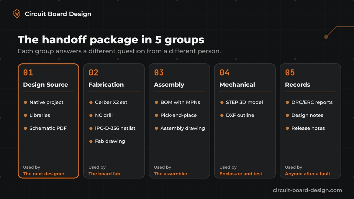
Fabs and tool vendors publish their own lists. Sierra Circuits asks for fab and assembly drawings, a BOM, an IPC netlist, Gerbers, NC drill and pick-and-place files. Altium's overview of output files covers the same ground from the designer's side. We sort everything into 5 groups, because each group is used by a different person on your team or in your supply chain.
| Group | Files | Who uses it | What breaks without it |
|---|---|---|---|
| 1. Design source | Native schematic and PCB project, symbol and footprint libraries, schematic PDF | You, or the next designer | Any change means redrawing the board |
| 2. Fabrication | Gerber X2 set with outline, NC drill, IPC-D-356 netlist, fab drawing with stackup | The bare board fab | Holds at CAM review, wrong stackup or finish |
| 3. Assembly | BOM with manufacturer part numbers, pick-and-place file, assembly drawing, paste layers | The assembler | Wrong parts, wrong rotation, quote delays |
| 4. Mechanical | STEP model of the assembled board, DXF outline, hole and keepout dimensions | Enclosure design and test fixtures | Board doesn't fit the case or the fixture |
| 5. Records | DRC and ERC reports, design notes and calculations, release notes | Anyone chasing a fault later | Nobody knows why a rule was waived |
What a release folder looks like
Here's a simple layout for one released revision, say rev B of a board released on 3 November 2026. The names are only an example. What matters is one folder per group and one revision label on everything.
board-revB-2026-11-03/01-source/native project, project libraries, schematic PDFboard-revB-2026-11-03/02-fab/Gerber X2 set, Excellon drill files, IPC-D-356 netlist, fab drawing PDF, ODB++ or IPC-2581 if askedboard-revB-2026-11-03/03-assembly/BOM (CSV or XLSX), pick-and-place CSV, assembly drawing PDFboard-revB-2026-11-03/04-mechanical/STEP model, DXF outlineboard-revB-2026-11-03/05-records/DRC and ERC reports, design notes, release notes
Keep a zipped copy somewhere you control, not behind a link that expires in 30 days.
1. Design source: native files and libraries
This is the group you should never sign off without. Native files are the editable project in the tool the board was drawn in. In Altium Designer that's the .PrjPcb project with its .SchDoc and .PcbDoc files. In KiCad it's the .kicad_pro, .kicad_sch and .kicad_pcb files.
Native files are only half of it. Your project also needs every symbol and footprint it uses. If those live in your designer's private library, the board can open on your machine with missing parts, or worse, with your own library's version of a part. Ask for the libraries packed with the project. Altium and KiCad can both put the parts a design uses into a project library.
Add a PDF of the schematic too. It's what you'll read on the bench at 11 pm. It must match the released revision exactly.
We deliver native files in either Altium Designer or KiCad. If you're still deciding which one you want to own, our Altium vs KiCad comparison covers the trade-offs, including file handoff. If your old boards are in EAGLE, see our EAGLE migration guide first.
2. Fabrication data: what the board fab needs
Your fab builds the bare board. It needs to know where copper goes, where holes go and what the board is made of. For a 4-layer board with parts on both sides, that's usually 11 Gerber files (4 copper, 2 mask, 2 paste, 2 silkscreen, 1 outline) plus 1 or 2 drill files.
- Gerber files. One file per copper, mask, paste and silkscreen layer, plus the board outline. Ask for Gerber X2. The Gerber format page from Ucamco explains that attributes tell the fab what each object is, such as an SMD pad, a via pad or a fiducial.
- NC drill files. Usually Excellon format. Plated and non-plated holes go in separate files, or they're clearly split in one.
- IPC-D-356 netlist. The fab compares it with the Gerbers and uses it for electrical test. It catches copper that doesn't match the design.
- Fab drawing or readme. Stackup, material, board thickness, copper weight, surface finish, mask and silkscreen colour, impedance targets and tolerances. A typical note reads something like "1.6 mm FR-4, 4 layers, 1 oz outer copper, ENIG, green mask, white silk, 90 ohm differential pairs on L1". Gerbers don't carry most of this.
Some fabs prefer a single structured file instead of a Gerber set. KiCad 9 can export Gerber, IPC-2581 and ODB++ from the PCB editor, and Altium can too. The IPC-2581 consortium describes its format as a standard for passing data from the designer to the fab and assembler.
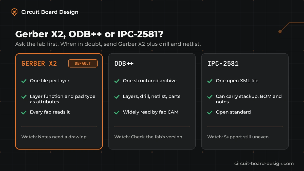
Ask your fab what it wants. If you don't know your fab yet, ask your designer for Gerber X2 plus drill and netlist, and a structured format as well if their tool can export it. It costs them a few minutes and you'll have both.
3. Assembly data: what the assembler needs
Your assembler places and solders the parts. They need to know which parts, where and which way round.
- BOM. One line per part with reference designators, quantity, value, package, manufacturer and manufacturer part number. Approved alternates help. Do-not-populate parts are marked the same way in the BOM, the schematic and the drawing.
- Pick-and-place file. Also called a centroid or XY file. It gives the position, rotation and side of every part. The origin must be stated.
- Assembly drawing. Top and bottom views with reference designators, pin 1 and polarity marks. It's what a person checks when a part looks wrong.
- Paste layers. Usually part of the Gerber set. The assembler uses them for the stencil.
A BOM with values but no manufacturer part numbers is a common gap. "10k 0402" isn't a part. It fits hundreds of parts with different tolerances. Somebody has to pick one, and if you don't, your assembler will choose what they have in stock. Altium's final deliverable checklist warns that part numbers are easy to forget when a design is revised.
4. Mechanical files
Your board has to fit something. Whoever designs your enclosure needs a STEP model of the assembled board with real part heights. It'll open in SolidWorks, Fusion or FreeCAD. A DXF of the outline with mounting holes and keepouts helps too. If you'll build a test fixture, its maker uses the same files to place probes on your test points.
5. Records: the files nobody asks for until something fails
These files explain the design. They're also the first thing you'll want when a board misbehaves 6 months after launch and the designer has moved on.
- DRC and ERC reports from the released revision. Every waived error needs a written reason.
- Design notes. Power budget, regulator calculations, impedance calculations, the stackup the fab confirmed and any layout rules taken from datasheets.
- Release notes. The revision, the date, what changed from the last revision and which files belong to it.
- Design review findings, if the board was reviewed. What was found, what was fixed and what was accepted. Our PCB design review checklist shows how we rank findings.
Red flags of a thin handoff
Most incomplete handoffs aren't bad faith. They come from a rush to get boards ordered. Here's what to watch for.
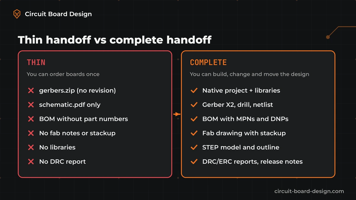
- Gerbers only. You can order the same board again. You can't change it, and you can't rerun a single design rule.
- A schematic PDF instead of the schematic. It's nice to read. You can't edit it or check it against the layout.
- Native files without libraries. Your project opens with missing symbols and footprints, or it pulls different parts from your own library.
- A BOM without manufacturer part numbers. Values and packages only. Your assembler picks the parts and you won't know which ones until you ask.
- No fab drawing or stackup. Your fab guesses or puts the job on hold. Your 90 ohm USB pair comes out at whatever the default stackup gives.
- Revisions that don't match. The silkscreen says rev A, the file names say rev C and the BOM has no revision at all.
- No DRC report, or waivers with no reason. You can't tell an accepted exception from a missed error.
- Outputs that don't match the source. The Gerbers came from an older version than the native files. Regenerate them from the native project and compare.
How to check a handoff in 30 minutes
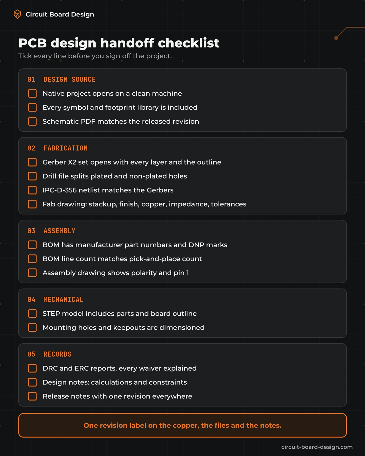
You don't need to be a layout engineer to run these checks. You need a computer that has never opened the project and about 30 minutes. We'd do it the day the files arrive.
- Open the native project on a clean machine. Use the same tool version the designer used. Check that no symbol or footprint is missing.
- Run DRC and ERC yourself. Compare the results with the reports you got. New errors mean the files and the reports don't match.
- Open the Gerbers in a viewer. GerbView, the free viewer that ships with KiCad, works for any tool's output. Check that every layer is there, nothing's mirrored and the outline is present.
- Count the parts. The number of placed parts in the pick-and-place file should equal the total quantity on the BOM, minus the DNP parts. Say your BOM adds up to 212 parts with 4 DNPs. Your placement file should list 208.
- Check one revision label everywhere. Copper or silkscreen, file names, BOM, fab drawing and release notes.
- Spot check 5 BOM lines. Look up each manufacturer part number on Octopart or a distributor site. Is it the right package? Is it still active? Is there stock?
- Ask for anything missing now. It's a 5-minute export for your designer while the project is fresh. In a year it may be a rebuild.
Put the deliverables list in the quote
The easiest time to get a complete package is before the work starts. Write the list into your quote or statement of work, so you and your designer agree on what "done" means. A short version is enough.
- Native files in a named tool and version, with project libraries.
- Fab package: Gerber X2, drill, IPC-D-356 netlist and fab drawing, plus ODB++ or IPC-2581 on request.
- Assembly package: BOM with manufacturer part numbers, pick-and-place and assembly drawing.
- STEP model and board outline.
- DRC and ERC reports, design notes and release notes for each released revision.
Who owns the files is a contract question, so check that part with your own lawyer. This list makes sure that what you own is something you can use.
Frequently asked questions
What files should a PCB designer deliver?
Five groups: the native design project with its libraries and a schematic PDF, fabrication data (Gerber X2, NC drill, IPC-D-356 netlist and a fab drawing), assembly data (BOM with manufacturer part numbers, pick-and-place and an assembly drawing), mechanical files (STEP model and outline) and records (DRC and ERC reports, design notes and release notes).
Are Gerber files enough?
Gerbers are enough to order the same bare board again. They are not enough to change the design, swap a part, move to another fab with different rules or fix a fault. For that you need the native project files with their libraries, plus the BOM and fab notes.
What are native PCB design files?
Native files are the editable project in the tool the board was drawn in, such as Altium Designer or KiCad. They hold the schematic, the layout, the nets and the design rules. Ask for them with the symbol and footprint libraries the project uses, so the design opens complete on any machine.
Should I ask for Gerber, ODB++ or IPC-2581?
Ask your fab first. Gerber X2 with drill files and an IPC-D-356 netlist is accepted almost everywhere. ODB++ and IPC-2581 put layers, drill, netlist and more into one structured file, which some fabs prefer. If the designer's tool exports both kinds, take both.
What should a PCB BOM include?
Reference designators, quantity, value, package, manufacturer and manufacturer part number for every line, with do-not-populate parts clearly marked. Approved alternates are a bonus. A BOM with values only, like "10k 0402", leaves the part choice to whoever builds the board.
Not sure your files are complete?
Send us your board and the files you received. Start with the free quick check and get checklist-level notes in 2 business days, no call needed. We'll tell you what's missing from the handoff and what we'd fix in the design. If you need more, you get a fixed quote per board before any work starts.
Send your board for a free quick check
Starting a new board? See our PCB layout and KiCad PCB design services, or contact us for a fixed quote. Every project ends with native files in Altium or KiCad.
Sources
- Sierra Circuits: PCB fabrication and assembly files
- Altium Resources: overview of PCB design outputs and manufacturing files
- Altium Resources: final deliverable checklist
- Ucamco: the Gerber format and Gerber X2 attributes
- IPC-2581 Consortium: IPC-2581 data transfer standard
- KiCad 9 documentation: PCB Editor fabrication outputs


